On-chip integrated ranging chip

A technology of chip and light detection, which is applied in the field of laser detection, can solve the problems of large size and achieve the effect of small size, easy large-scale integration and high integration

Pending Publication Date: 2022-01-21
CHINA SCI PHOTON CHIP HAINING TECH CO LTD
View PDF0 Cites 0 Cited by
  • Summary
  • Abstract
  • Description
  • Claims
  • Application Information

AI Technical Summary

Problems solved by technology

[0004] Therefore, the technical problem to be solved by the present invention is to overcome the defect of large size of the existing laser ranging system, thereby providing an on-chip integrated ranging chip

Method used


Image

  • On-chip integrated ranging chip
  • On-chip integrated ranging chip
  • On-chip integrated ranging chip

Examples


Embodiment 1

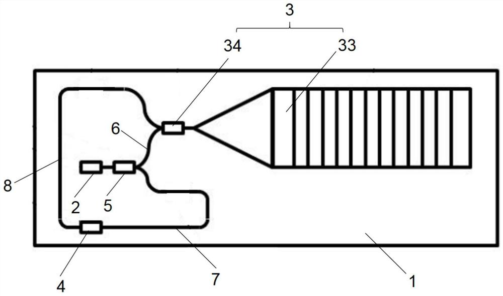
[0039] see figure 1 , the present embodiment provides an on-chip integrated ranging chip, including: a semiconductor substrate 1; a laser emitting element 2 arranged on one side surface of the semiconductor substrate 1, a detection and reception diffraction structure 3 and an analysis module 4, the The detection and receiving diffraction structure 3 is adapted to receive the laser signal output by the laser emitting part 2, emit the laser signal to the target object, and receive the laser signal reflected by the target object, and the analysis module 4 is adapted to obtain the laser signal time-of-flight and calculate the distance of the target object according to the time-of-flight.

[0040] In the above-mentioned on-chip integrated distance measuring chip, the laser signal emitted by the laser emitting part 2, the detection and receiving diffraction structure 3 receives the laser signal output by the laser emitting part 2 and then emits the laser signal to the target object,...

Embodiment 2

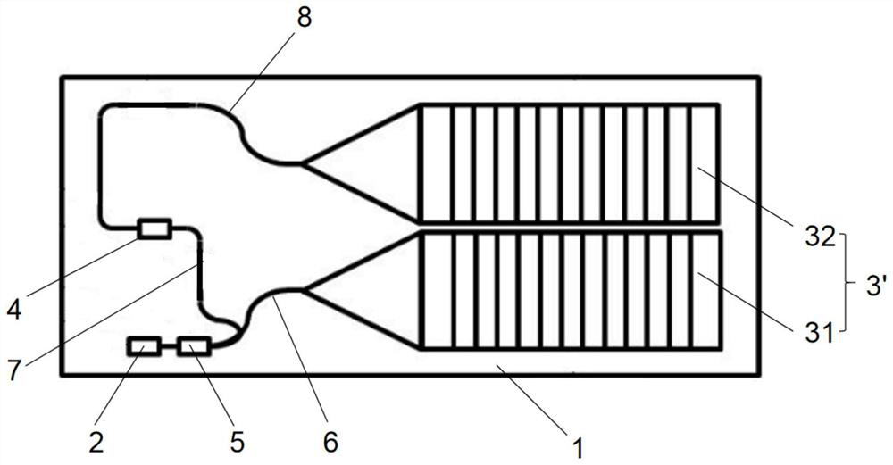
[0053] see figure 2 , this embodiment provides an on-chip integrated ranging chip, which differs from the on-chip integrated ranging chip provided in Embodiment 1 in that:

[0054] The detection and reception diffraction structure 3' includes a transmission diffraction unit 31 and a reception diffraction unit 32 spaced apart from each other, the transmission diffraction unit 31 is connected to the output end of the detection light transmission member 6, and the transmission diffraction unit 31 is suitable for sending The target emits the laser signal, the receiving diffraction unit 32 is connected to the input end of the echo transmission member 8 , and the receiving diffraction unit 32 is adapted to receive the laser signal reflected by the target. The detecting and receiving diffraction structure 3' separates the emission and reception of the laser signal, so that the emission and reception of the laser signal do not affect each other, so the emission and reception of the l...

Embodiment 3

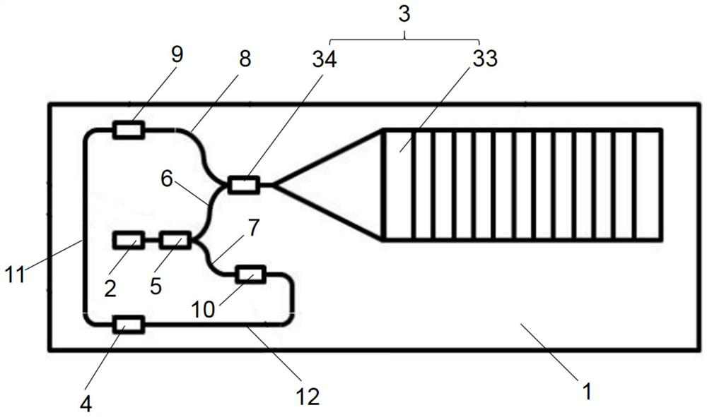
[0058] see image 3, the present embodiment provides an on-chip integrated ranging chip, including: a semiconductor substrate 1; a laser emitting element 2 arranged on one side surface of the semiconductor substrate 1, a detection and reception diffraction structure 3 and an analysis module 4, the The detection and receiving diffraction structure 3 is adapted to receive the laser signal output by the laser emitting part 2, emit the laser signal to the target object, and receive the laser signal reflected by the target object, and the analysis module 4 is adapted to obtain the laser signal time-of-flight and calculate the distance of the target object according to the time-of-flight.

[0059] In this embodiment, the material of the semiconductor substrate 1 includes, but is not limited to, III-V group semiconductor materials and silicon-based materials. In this embodiment, the laser emitting element 2 and the analysis module 4 are respectively fixed on the surface of the semic...


PUM


Abstract

The invention provides an on-chip integrated ranging chip. The on-chip integrated ranging chip comprises a semiconductor substrate; a laser emitting part, a detection receiving diffraction structure and an analysis module, arranged on the surface of one side of the semiconductor substrate. The detection receiving diffraction structure is suitable for receiving a laser signal output by the laser emitting part, emitting a laser signal to a target object, receiving a laser signal reflected by the target object and analyzing the laser signal to the target object. The analysis module is suitable for obtaining the flight time of the laser signal and calculating the distance of the target object according to the flight time. The on-chip integrated ranging chip can detect, track and identify a target object, has a small size and a high integration level, solves the problem that a laser ranging system is large in size, and facilitates large-scale integration.

Description

technical field [0001] The invention relates to the technical field of laser detection, in particular to an on-chip integrated ranging chip. Background technique [0002] Laser ranging technology is a technology that detects the position, speed and other characteristic quantities of the target by emitting laser light. The currently commonly used ranging scheme is Time of Flight (TOF for short), and its working principle is to transmit a detection signal to the target and receive the echo signal reflected by the target, so as to obtain the flight time of the detection signal, and then Obtain the relevant information of the target, so as to detect, track and identify the target. The time-of-flight method has the advantages of small error and relatively stable performance. At present, the laser ranging system includes a laser transmitter, an optical receiver and an information processing component. The laser transmitter is used to transmit detection signals, the optical recei...

Claims


Application Information

Patent Timeline
Patent Type & Authority Applications(China)
IPC IPC(8): G01S17/10G01S7/4865G01S7/484G01S7/481
CPCG01S17/10G01S7/484G01S7/4865G01S7/4811
Inventor 刘敬伟徐浩李文玲
Owner CHINA SCI PHOTON CHIP HAINING TECH CO LTD
Why Eureka
Try Eureka