Wireless signal processing method and system applying all-programmable system on chip
A system-on-chip, wireless signal technology, applied in transmission systems, electrical digital data processing, programming languages/paradigms, etc., can solve problems such as poor system stability, large system size, and complex equipment, and achieve high practicability and high-level development. Efficient and practical effect
- Summary
- Abstract
- Description
- Claims
- Application Information
AI Technical Summary
Problems solved by technology
Method used
Image
Examples
Embodiment 1
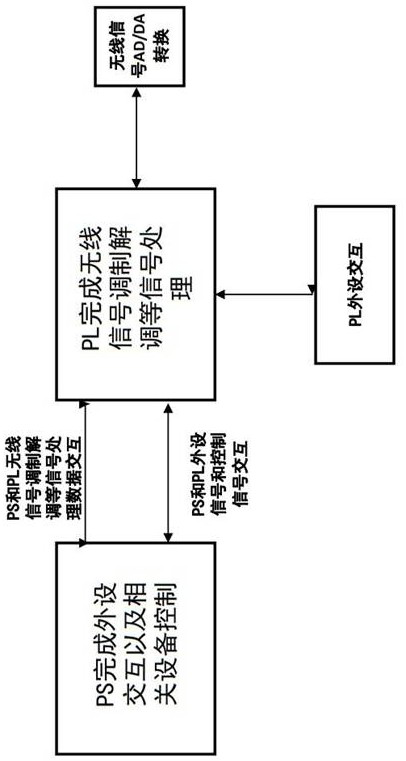
[0037] Such as Figure 1 to Figure 6 As shown, compared with the traditional CPLD, FPGA has the advantages of shortened development cycle, simplified logic, and lower cost for wireless signal processing. Among them, Xilinx Zynq 7000 series (preferably Zynq 7000) products integrate the processing system (Processing System, PS) of the dual-core ARM-Cortex-A9 MPCore processor with the programmable logic (Pro-grammable Logic, PL) system of programmable logic resources Integrated embedded system hardware design. The present invention is based on the Xilinx Zynq 7000 series platform in combination with signal processing features and Zynq 7000 series platform characteristics to carry out the design of the signal processing architecture, and utilize the respective characteristics of PL and PS to design the wireless signal processing architecture method as follows figure 1 .
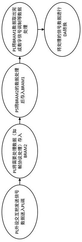
[0038] The two BRAMs of the Zynq 7000 series are named BRAM1 and BRM2 respectively. The processing of wirel...
Embodiment 2
[0049] Such as Figure 1 to Figure 6 As shown, as a further optimization of Embodiment 1, this embodiment includes all the technical features of Embodiment 1. In addition, this embodiment also includes the following technical features:
[0050] Reception: The wireless signal received by the wireless channel antenna is converted by AD, and the data is transmitted to the PL, and the signal processing process such as demodulation is completed in the PL, and the data is stored in BRAM1, and the PS takes out the BRAM1 data for corresponding processing.
[0051] Sending: The original data sent by the belt is transmitted to PL through serial port 1, PL stores the data into BRAM2, PS takes the data out from BRAM2 for corresponding processing, stores the processed data into BRAM1, PL takes out the data of BRAM1 for modulation and other signals Processing, and then the data is processed by DA and sent out. While performing sending processing, PS will control RF commands to be transmitt...
PUM
 Abstract
Description
Claims
Application Information


