
Method for producing semiconductor device

A semiconductor and device technology, applied in the field of semiconductor device production, can solve problems such as incomplete electrical connection and conductive disconnection of lower and upper interconnects 302 and 307

Inactive Publication Date: 2004-02-25
RENESAS ELECTRONICS CORP
View PDF0 Cites 0 Cited by
  • Summary
  • Abstract
  • Description
  • Claims
  • Application Information

AI Technical Summary

Problems solved by technology

[0008] In the conventional method, although the natural oxide film on the lower interconnect 302 on the bottom surface of the via hole 305 is removed, in some cases, the lower and upper interconnects 302 and 307 are not completely electrically connected.
This is because the connection through the via 305 would be defective, causing a conductive disconnection between the lower interconnect 302 and the plug 306.

Method used


Image

  • Method for producing semiconductor device
  • Method for producing semiconductor device
  • Method for producing semiconductor device

Examples


no. 1 example

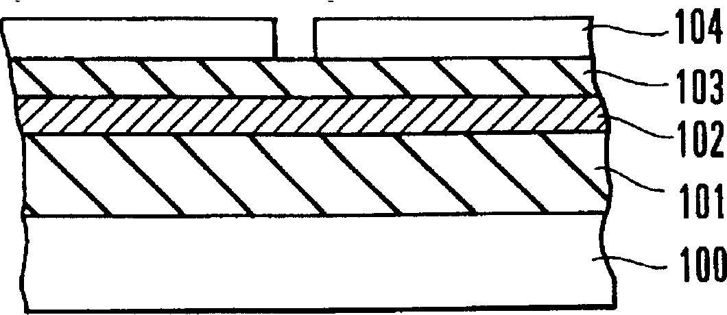
[0024] First, if Figure 1A As shown, a predetermined element (not shown), a wiring layer (not shown) to be distributed on the element, and the like are formed on a semiconductor substrate 100, and an interlayer insulating film 101 is formed to cover the semiconductor substrate 100. surface. Then, lower interconnect 102 made of aluminum is formed on interlayer insulating film 101 .

[0025] Such as Figure 1B As shown, an interlayer insulating film 103 is formed on an interlayer insulating film 101 including a lower interconnection 102, and a protective pattern 104 having an opening is formed on the interlayer insulating film 103 on the lower interconnection 102 by using a known photolithography technique.

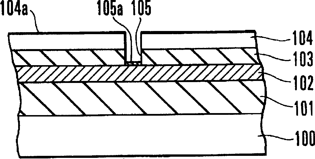
[0026] Such as Figure 1C As shown, by using the resist pattern 104 as a mask, the interlayer insulating film 103 is selectively etched by dry etching (reactive ion etching) using a fluorine-containing gas, thereby forming a via hole 105 . More specifically, fluorinate...

no. 2 example

[0035]The case where a conductive antireflection film is formed on a metal wiring layer (for example, an aluminum layer) will be described below. When the degree of microfabricated patterns increases, when forming fine interconnection patterns by photolithography, anti-reflection patterns are used to suppress light reflection of the bottom layer.

[0036] First, if Figure 2A As shown, a predetermined element (not shown), a wiring layer (not shown) to be distributed on the element, and the like are formed on a semiconductor substrate 200, and an interlayer insulating film 201 is formed to cover the semiconductor substrate 200. surface. Then, lower interconnection 202 made of aluminum is formed on interlayer insulating film 201 . A conductive anti-reflection coating 202 a is formed on the lower interconnect 202 . Figure 2A A cross-sectional view of the lower interconnection 202 in the width direction is shown.

[0037] Such as Figure 2B As shown, an interlayer insulating...


PUM


Abstract

In a method of manufacturing a semiconductor device, in the first step, a lower interconnection is formed on a semiconductor substrate through a first interlevel insulating film. In the second step, a second interlevel insulating film is formed on the semiconductor substrate including the lower interconnection. In the third step, a through hole is formed in the second interlevel insulating film to reach the lower interconnection. In the fourth step, after the third step is ended, a surface of the lower interconnection including a side surface thereof exposed to a bottom portion of the through hole is etched without exposing the semiconductor substrate to the atmosphere. In the fifth step, a plug made of a conductive material is formed in the through hole. In the sixth step, an upper interconnection to be connected to the plug is formed on the second interlevel insulating film.

Description

technical field [0001] The present invention relates to a method of producing a semiconductor device having a multilayer interconnection structure. Background technique [0002] Due to the high integration, high density, and high operating speed and versatility of LSIs (Large Scale Integrated Circuits), a multilayer interconnection structure is an indispensable technology not only in logic devices but also in large-scale memory devices. The multilayer interconnection structure can reduce the interconnection area, greatly reduce the increase of the chip area, and shorten the average interconnection length to suppress the delay of the working speed caused by the interconnection resistance. [0003] In this multilayer interconnect structure technology, it is important to reliably connect wiring layers to each other. In particular, connection technology in a large number of fine via holes is important in VLSI. When aluminum is used as a wiring material, an oxide film usually e...

Claims


Application Information

Patent Timeline
IPC IPC(8): H01L21/28H01L21/302H01L21/3065H01L21/3205H01L21/768H01L23/52H01L23/522
CPCH01L21/76802H01L23/5226H01L2924/0002H01L2924/00H01L21/768
Inventor 小川博
Owner RENESAS ELECTRONICS CORP
Learn More