A pin-cutting device for high-power field effect transistors

A field-effect transistor and cutting device technology, which is applied in semiconductor/solid-state device manufacturing, electrical components, circuits, etc., can solve the problems of low production efficiency, waste of manpower, single mechanism, etc., and achieve the effect of saving manpower and improving production efficiency

Active Publication Date: 2022-08-09
先之科半导体科技(东莞)有限公司
View PDF8 Cites 2 Cited by
  • Summary
  • Abstract
  • Description
  • Claims
  • Application Information

AI Technical Summary

Problems solved by technology

[0003] In general field effect transistor body production, in order to ensure different installation environments, the pins will be made longer, but in actual use, the longer pins bring some inconvenience to the installation, which affects the installation of field effect transistors. For work efficiency on the circuit board, longer pins need to be cut to a suitable length
The traditional pin cutting device has a single mechanism, and most of them manually place field effect transistors to cut pins in sequence, resulting in low production efficiency and waste of manpower. Therefore, a high-power field effect transistor pin cutting device is needed to solve the above problems

Method used


Image

  • A pin-cutting device for high-power field effect transistors
  • A pin-cutting device for high-power field effect transistors
  • A pin-cutting device for high-power field effect transistors

Examples


Embodiment Construction

[0047] In order to further understand the features, technical means, and specific goals and functions of the present invention, the present invention will be described in further detail below with reference to the accompanying drawings and specific embodiments.

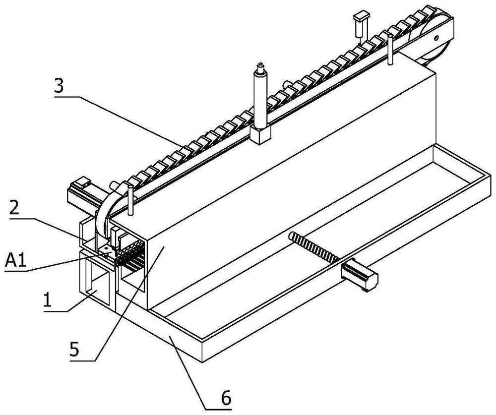
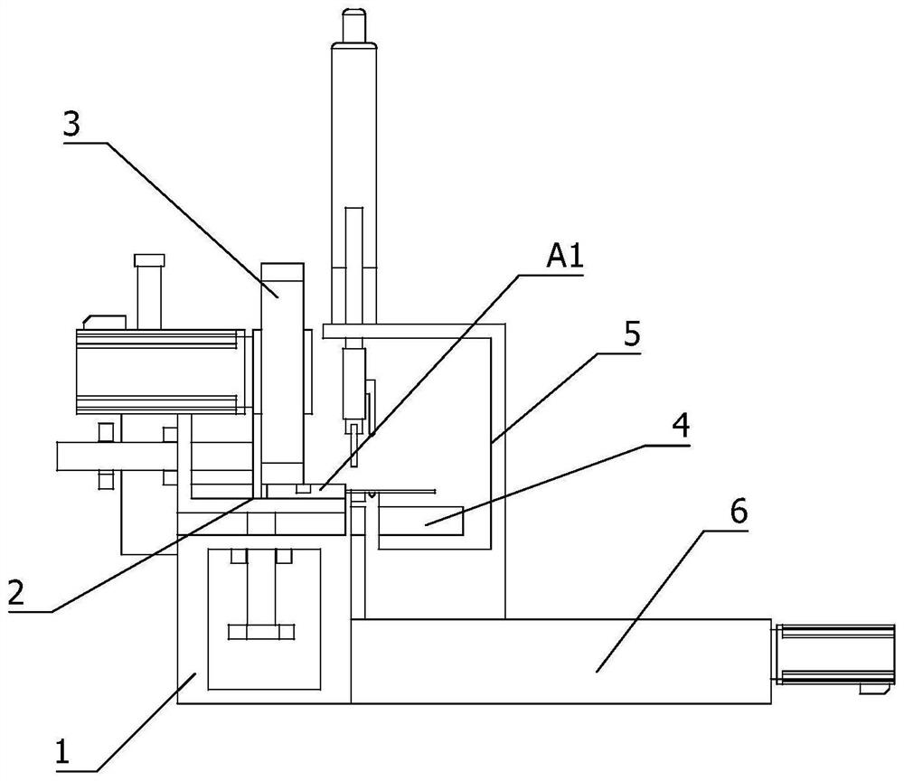
[0048] like figure 1 and 2 shown:

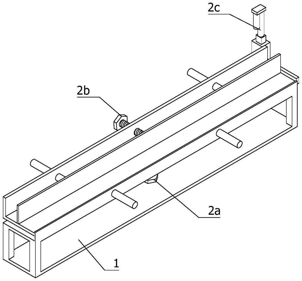
[0049] A pin cutting device for high-power field effect transistors, comprising a bracket 1, a transistor limit arrangement device 2, a conveying device 3, a guide column 4, a pin carding and cutting device 5 and a ball screw slide table 6; transistor limit arrangement The device 2 is fixedly installed on the bracket 1; the conveying device 3 is fixedly installed on the transistor limit arrangement device 2; the ball screw slide table 6 is arranged beside the bracket 1; The carding and cutting device 5 is fixedly connected with the working end of the ball screw slide table 6; the guide column 4 is provided with several symmetrically arranged on the side of the bracket 1, one end o...


PUM


Abstract

The invention relates to the technical field of field effect transistor production, in particular to a pin cutting device for high-power field effect transistors, comprising a bracket, a transistor limiting arrangement device, a conveying device, a guide column, a pin carding and cutting device and a ball screw The sliding table; the transistor limit arrangement device is fixedly installed on the bracket; the conveying device is fixedly installed on the transistor limit arrangement device; the ball screw sliding table is arranged beside the bracket; The cutting device is fixedly connected with the working end of the ball screw slide table; the guide column is provided with several symmetrically arranged on the side of the bracket, one end of the guide column is fixedly connected with the bracket, and the end of the guide column away from the bracket slides and extends through the pin combing and cutting device. The present application can effectively save manpower and at the same time improve production efficiency.

Description

technical field [0001] The invention relates to the technical field of field effect transistor production, in particular to a pin cutting device of a high-power field effect transistor. Background technique [0002] Semiconductors refer to materials with electrical conductivity between conductors and insulators at room temperature. Semiconductors are used in integrated circuits, consumer electronics, communication systems, photovoltaic power generation, lighting, high-power power conversion and other fields. For example, field effect transistors are made of semiconductors. From the perspective of technology or economic development, the importance of semiconductors is very huge. Most electronic products, such as computers, mobile phones, or the core units of digital recorders, are closely related to semiconductors. [0003] In general, when making field effect transistors, in order to ensure different installation environments, the pins will be made longer. In actual use, th...

Claims


Application Information

Patent Timeline
Patent Type & Authority Patents(China)
IPC IPC(8): B21F11/00B21F23/00H01L21/67
CPCB21F11/00B21F23/005H01L21/67092
Inventor 蒋发坤
Owner 先之科半导体科技(东莞)有限公司
Why Eureka
Try Eureka