
LCOS (Liquid Crystal On Silicon) surface micro-support structure and processing method thereof

A support structure and processing method technology, applied in nonlinear optics, static indicators, optics, etc., can solve the problems of inability to effectively improve the thickness of the cell, prone to agglomeration, uncontrollable, etc., to improve the thickness of the liquid crystal cell and improve the structural stability performance and image quality, reducing the effect of

Inactive Publication Date: 2022-02-15
南京数字光芯科技有限公司
View PDF5 Cites 0 Cited by
  • Summary
  • Abstract
  • Description
  • Claims
  • Application Information

AI Technical Summary

Problems solved by technology

[0003] The thickness of the current liquid crystal cell is generally several hundred nanometers to several microns. When the LCOS size is large, it is easy to deform, so it is difficult to ensure the uniformity of the cell thickness. In the prior art, glass beads are used to improve the thickness of the liquid crystal cell. The solution, small glass beads are very convenient to process, but the disadvantage is that the distribution of glass beads is scattered and uncontrollable, and they are prone to agglomeration, resulting in some places without support, which still cannot effectively improve the thickness of the box and reunite together Glass beads can affect pixel deflection

Method used


Image

  • LCOS (Liquid Crystal On Silicon) surface micro-support structure and processing method thereof
  • LCOS (Liquid Crystal On Silicon) surface micro-support structure and processing method thereof
  • LCOS (Liquid Crystal On Silicon) surface micro-support structure and processing method thereof

Examples


Embodiment Construction

[0029] The following will clearly and completely describe the technical solutions in the embodiments of the present invention with reference to the accompanying drawings in the embodiments of the present invention. Obviously, the described embodiments are only some, not all, embodiments of the present invention. Based on the embodiments of the present invention, all other embodiments obtained by persons of ordinary skill in the art without making creative efforts belong to the protection scope of the present invention.

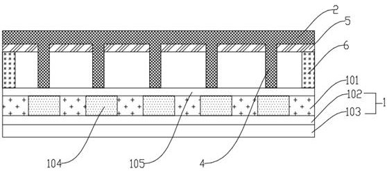
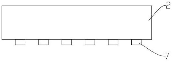
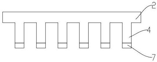
[0030] refer to figure 1 As shown, the first specific implementation of this embodiment is a micro-support structure 4 on the surface of LCOS, including a CMOS substrate 1, a packaging substrate 2, an alignment layer and a liquid crystal layer 3 arranged between the two, and the packaging substrate 2 is provided with a transparent electrode 5 (cathode conductive material, generally ITO) on the side close to the alignment layer, and a metal electrode 101 is pro...


PUM


Abstract

The invention discloses an LCOS surface micro-support structure and a processing method thereof. The LCOS surface micro-support structure comprises a CMOS substrate, a packaging substrate and an orientation layer arranged between the CMOS substrate and the packaging substrate, wherein a transparent electrode is arranged on one side, close to the orientation layer, of the packaging substrate, a metal electrode is arranged on one side, close to the orientation layer, of the CMOS substrate, the metal electrode is used for reflecting incident light and forming conduction potential between the metal electrode and the transparent electrode, the orientation layer comprises an initial state and a deflection state, when the orientation layer is in the initial state, the polarization direction of the incident light is not changed, and when the orientation layer is in a deflection state, the polarization direction of incident light passing through the orientation layer is rotated by 90 degrees, a micro-supporting structure is arranged between the CMOS substrate and the packaging substrate, the micro-supporting structure is arranged at an intersection point of a plurality of metal electrodes, thickness of a liquid crystal box of the LCOS can be effectively improved through the arrangement of the micro-supporting structure, and structural stability and imaging quality of the LCOS are improved.

Description

technical field [0001] The invention relates to the technical field of LCOS silicon-based liquid crystals, in particular to an LCOS surface micro-support structure and a processing method thereof. Background technique [0002] At present, the requirement for liquid crystal on silicon devices (LCOS) is that the uniformity of the thickness of the liquid crystal cell should be relatively consistent, so as to ensure better imaging quality. A fringe field effect is generated between pixels, which has a serious adverse effect on the phase modulation depth and diffraction efficiency of the LCOS cell. However, the fringe field effect of the LCOS is related to the ratio of the width of the pixel electrode to the thickness of the liquid crystal cell. The smaller the ratio, the adjacent The stronger the fringe field effect between pixels, the liquid crystal deflection is directly related to the thickness of the cell, and the thickness of the cell directly affects the imaging quality. ...

Claims


Application Information

Patent Timeline
Patent Type & Authority Applications(China)
IPC IPC(8): G02F1/133G02F1/1333G02F1/1339G02F1/1341G02F1/1343
CPCG02F1/13394G02F1/13306G02F1/134309G02F1/1341G02F1/1333
Inventor 孙雷张婧姣
Owner 南京数字光芯科技有限公司
Learn More