
Eureka
For R&D, Eureka makes reading and utilizing patents & technical documents easy.
Eureka AIR
Designed for self-driven R&D workflows. Generate viable solutions, solve complex R&D challenges, empower your innovation with AI.

Eureka Materials
Designed for material experts only. Revolutionize your material R&D, from search, analyze, to developing new materials.

TechResearch
Generate reliable direction feasibility study reports for your R&D in just a few steps.

TechSeek
Discover and master advanced knowledge NOW. Basics, ideas, possibilities, all at once.

TechMind
As an expert in R&D Theories, TechMind can generates customized viable solutions instantly.

TechRisk
Analyze your overall solution with one click, know your potential R&D risks in advance.

TechMonitor
Get weekly tech updates, stay abreast of the latest tech innovations and key insights.
Chip, chip optimization method and electronic equipment
A chip and sub-module technology, applied in the field of chips, chip optimization methods and electronic equipment, can solve the problems of related circuit failure, chip performance reduction, chip failure, etc., and achieve the effect of increasing the number of settings, improving the availability rate, and increasing the number
- Summary
- Abstract
- Description
- Claims
- Application Information
AI Technical Summary
Problems solved by technology
Method used
Image

Examples
no. 1 example
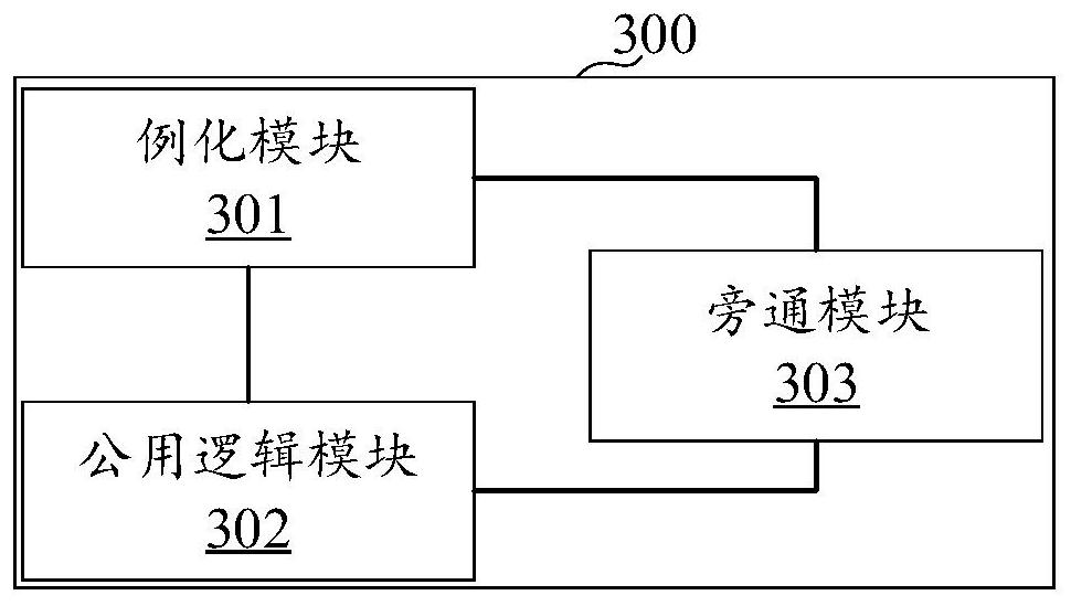
[0041] see figure 1 , the embodiment of the present invention provides a chip 300, including: an instantiation module 301, a common logic module 302 and a bypass module 303, wherein the instantiation module 301 and the common logic module 302 are connected, and the instantiation module 301 is also connected through the bypass module 303 is connected to the common logic module 302 .
[0042] The instantiation module 301 is configured to realize preset processing functions. Specifically, the instantiation module 301 includes multiple identical instantiation units, and each instantiation unit can implement a corresponding function or logic. The preset processing function is determined by the type of the chip 300, which is well known to those skilled in the art, and will not be described in detail in this embodiment.
[0043]The working mode realized by each instantiation unit in the instantiation module 301 in this embodiment is similar to a large number of repeated units in th...
no. 2 example
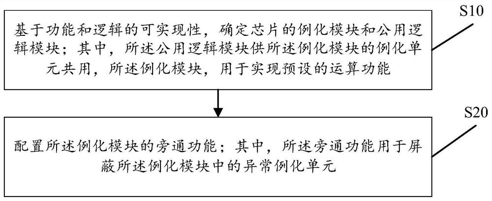
[0058] see image 3 , A chip optimization method is provided in the embodiment of the present invention. For the relevant explanation and meaning of the terms in this embodiment, please refer to the above-mentioned first embodiment. Specifically, the method includes:
[0059] Step S10: Based on the realizability of functions and logic, determine the instantiation module and common logic module of the chip; wherein, the common logic module is shared by the instantiation unit of the instantiation module, and the instantiation module is used for Realize the preset processing function.
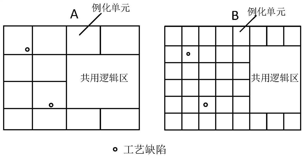
[0060] In step S10, when determining the instantiation module of the chip, the logic that can be shared in the instantiation unit in the instantiation module should be separated as much as possible to form a separate common logic module. Thus, the instantiation module and the common logic module are divided into two area settings, the instantiation area and the common logic area. Since the commo...
no. 3 example
[0075] Based on the same inventive concept, this embodiment also provides an electronic device, including a processor and a memory, the memory is coupled to the processor, the memory stores instructions, and when the instructions are executed by the processor During execution, the electronic device is made to execute the steps of any one of the methods in the above-mentioned second embodiment.
[0076] It should be noted that, in the electronic device provided by the embodiment of the present invention, when the instructions are executed by the processor, the specific implementation and technical effects of each step are the same as those of the foregoing method embodiments. For a brief description, this For the parts not mentioned in the embodiments, reference may be made to the corresponding content in the foregoing method embodiments.
PUM
 Abstract
Description
Claims
Application Information
 - R&D Engineer
- R&D Manager
- IP Professional
- Industry Leading Data Capabilities
- Powerful AI technology
- Patent DNA Extraction
Browse by: Latest US Patents, China's latest patents, Technical Efficacy Thesaurus, Application Domain, Technology Topic, Popular Technical Reports.
© 2024 PatSnap. All rights reserved.Legal|Privacy policy|Modern Slavery Act Transparency Statement|Sitemap|About US| Contact US: help@patsnap.com