Supercharge Your Innovation With Domain-Expert AI Agents!

Silicon wafer laser marking method and system, and computer equipment

A laser marking and silicon wafer technology, applied in laser welding equipment, welding equipment, metal processing equipment, etc., can solve the problems of dust particles, difficult to identify, unclear appearance, etc., to ensure cleanliness, reduce pollution, and clear appearance Effect

Pending Publication Date: 2022-02-22
HANS LASER TECH IND GRP CO LTD
View PDF5 Cites 0 Cited by
  • Summary
  • Abstract
  • Description
  • Claims
  • Application Information

AI Technical Summary

Problems solved by technology

[0003] The embodiment of the present invention provides a silicon wafer laser marking method, system and computer equipment, which solves the problems in the prior art that dust particles appear around the identification code after laser, the appearance is unclear and difficult to identify

Method used


Image

  • Silicon wafer laser marking method and system, and computer equipment
  • Silicon wafer laser marking method and system, and computer equipment
  • Silicon wafer laser marking method and system, and computer equipment

Examples


Embodiment Construction

[0016] The following will clearly and completely describe the technical solutions in the embodiments of the present invention with reference to the accompanying drawings in the embodiments of the present invention. Obviously, the described embodiments are some of the embodiments of the present invention, but not all of them. Based on the embodiments of the present invention, all other embodiments obtained by persons of ordinary skill in the art without creative efforts fall within the protection scope of the present invention.

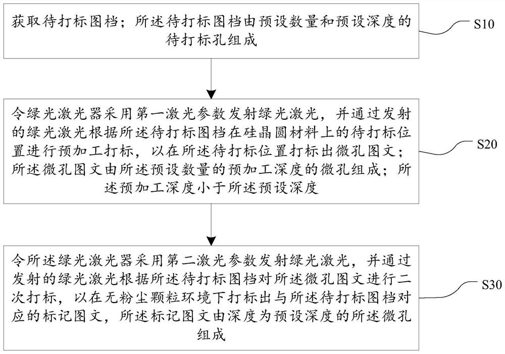
[0017] The invention provides a silicon wafer laser marking method, such as figure 1 shown, including the following steps:

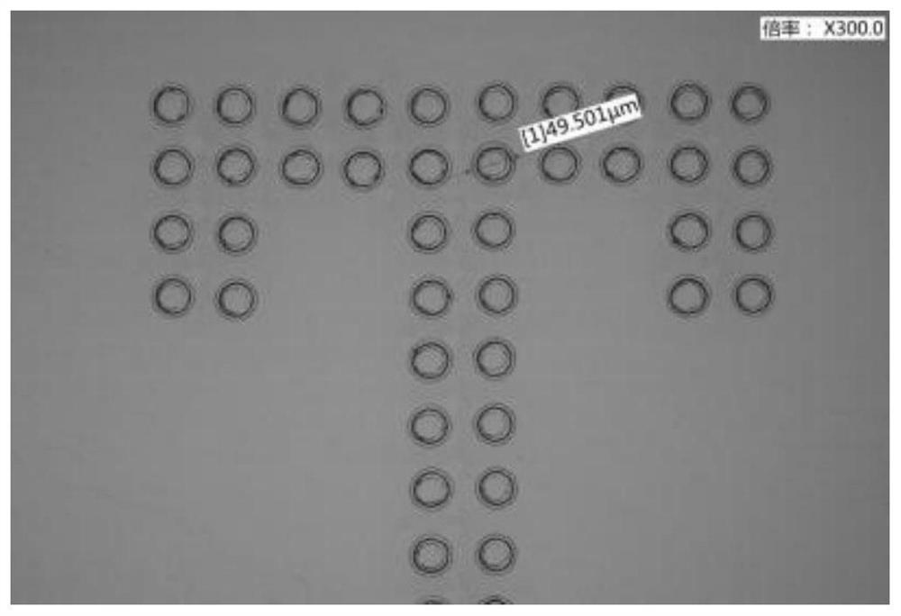
[0018] S10. Obtain the image file to be marked; the image file to be marked is composed of holes to be marked with a preset number and depth; wherein, the image file to be marked is composed of holes to be marked, optional Specifically, the holes to be marked in the image file to be marked are all round holes with the same diame...


PUM

PropertyMeasurementUnit
Wavelengthaaaaaaaaaa
Pulse widthaaaaaaaaaa
Diameteraaaaaaaaaa

Abstract

The invention discloses a silicon wafer laser marking method and system, and computer equipment. The silicon wafer laser marking method comprises the following steps: acquiring a to-be-marked drawing file; enabling a green laser to emit a green laser according to the first laser parameter, and carrying out preprocessing marking on the to-be-marked position on the silicon wafer material according to the to-be-marked drawing file through the emitted green laser so as to mark a micropore image-text at the to-be-marked position, wherein the micropore image-text is composed of a preset number of micropores with pre-processing depth; and enabling the green laser to emit the green laser according to the second laser parameter, carrying out secondary marking on the micropore image-text through the emitted green laser according to the to-be-marked image-text so that a marked image-text corresponding to the to-be-marked image-text is marked in the dust-free particle environment, wherein the marked image-text is composed of micropores with the preset depth. The method is high in flexibility, free of pollution and good in stability, micropores in marked images and texts are clear in appearance, free of particle dust pollution and not prone to being covered, and identifiability of the marked images and texts is guaranteed.

Description

technical field [0001] The invention relates to the field of laser processing, in particular to a silicon wafer laser marking method, system and computer equipment. Background technique [0002] Silicon material is a material widely used in the semiconductor industry among the currently known materials. It occupies an extremely important position in the semiconductor industry and is widely used in components such as integrated circuits, IC chips, detectors, and diodes. With the miniaturization, multi-function and intelligentization of electronic devices, the volume of integrated circuit packaging devices is reduced in three dimensions. In order to effectively trace the production process in the process of making chips, laser processing technology will be used to perform laser formation on the surface of silicon wafers. The identification code, and then track the manufacturing, testing and other processes of each silicon wafer through the identification code. In the prior ar...

Claims


Application Information

Patent Timeline
IPC IPC(8): B23K26/362B23K26/382H01L21/67
CPCB23K26/362B23K26/382H01L21/67282Y02P70/50
Inventor 林家新焦波温尧明谢圣君吕启涛高云峰
Owner HANS LASER TECH IND GRP CO LTD
Features
  • R&D
  • Intellectual Property
  • Life Sciences
  • Materials
  • Tech Scout
  • Unparalleled Data Quality
  • Higher Quality Content
  • 60% Fewer Hallucinations
Learn More