Wafer test probe station with high performance and high efficiency
A Wafer Test, High Efficiency Technology
- Summary
- Abstract
- Description
- Claims
- Application Information
AI Technical Summary
Problems solved by technology
Method used
Image

Examples
Embodiment Construction
[0024] In order to make the techniques, creative characteristics of the present invention, it is easy to understand that the present invention is further illustrated in connection with the specific embodiments.
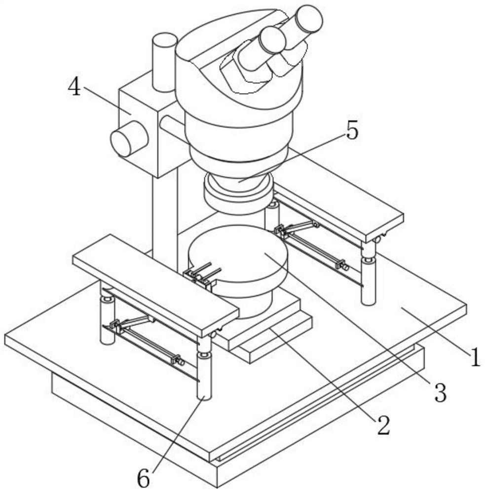
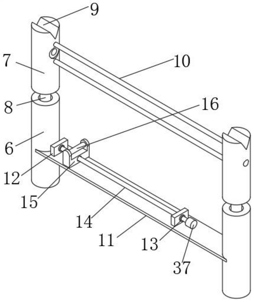
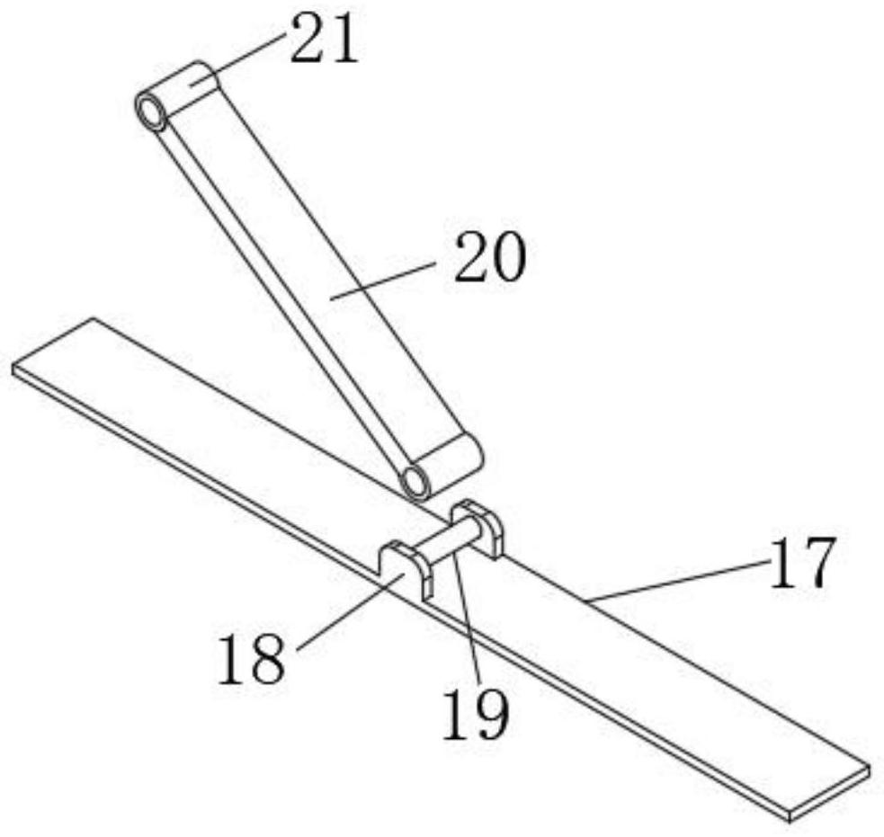
[0025] Such as Figure 1-6 As shown, a wafer test probe station having high performance high-performance, including the No. 1 mounting table 1, a lateral longitudinal adjustment stage 2, and the lateral longitudinal adjustment stage 2 is provided with a table 3 The rear side position of the table 3 is provided with a rear bracket 4, and the rear bracket 4 is provided with a viewing mirror barrel 5, and the first mounting table 1 is provided with a side lower mounting tube 6 on both sides of the table 3. The internal movable rod 8 is provided in the side lower mounting tube 6, and the upper end position of the inner movable rod 8 is provided with a side mounting column 7, and the lower mounting plate 11 is provided between the side surface mount 6, and the lower mounting pl...
PUM
 Abstract
Description
Claims
Application Information