Display panel and manufacturing method thereof

A display panel and top surface technology, which is applied in semiconductor/solid-state device manufacturing, instruments, electrical components, etc., can solve problems such as easy peeling, TFT arrangement influence, large hollowing out of flat areas, etc., to reduce interlayer peeling Probability, effect of improving structural stability

Pending Publication Date: 2022-03-01
BOE TECH GRP CO LTD
View PDF1 Cites 0 Cited by
  • Summary
  • Abstract
  • Description
  • Claims
  • Application Information

AI Technical Summary

Problems solved by technology

[0002] With the development of display technology, flexible display devices have appeared in the market for folding screens. Compared with traditional display devices, folding screens have significant advantages. Peeling, shedding problem
An important reason for the current failure is that the adhesion between the layers of the organic light-emitting material using the evaporation process is weak. During the repeated bending process, the long-term shear stress will cause the peeling between the layers to cause the device to fail.
[0003] The Chinese patent application with the application number CN202010937199.6 discloses a display panel and its manufacturing method. An undercut structure is added to the backplane to form a pinning structure between the inorganic layer and the substrate, but the pinning structure is set on the thin film transistor. In the SD layer, it is necessary to borrow the SD layer, which causes a spatial squeeze on the TFT structure on the backplane, affects the TFT arrangement, and hollows out the flat area too much, which seriously affects the subsequent inkjet printing encapsulation layer. Leveling

Method used


Image

  • Display panel and manufacturing method thereof
  • Display panel and manufacturing method thereof
  • Display panel and manufacturing method thereof

Examples


Embodiment Construction

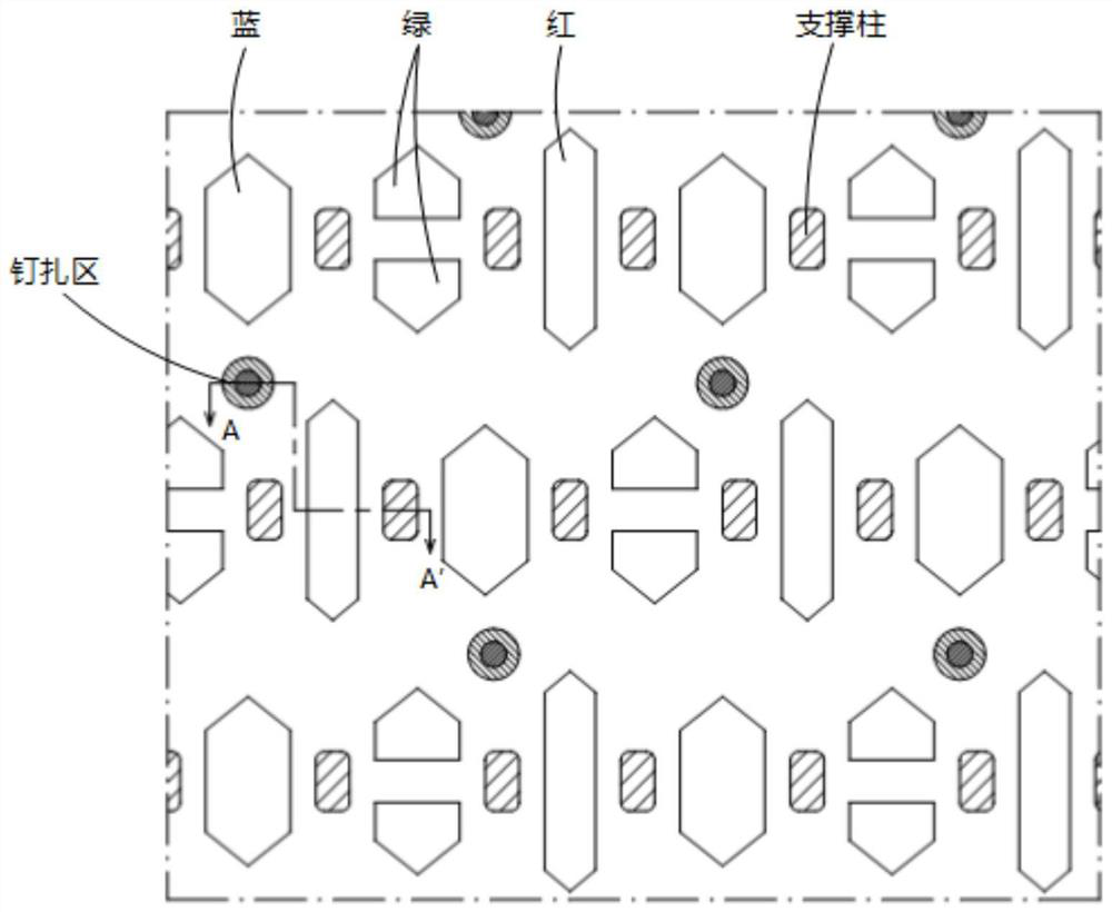
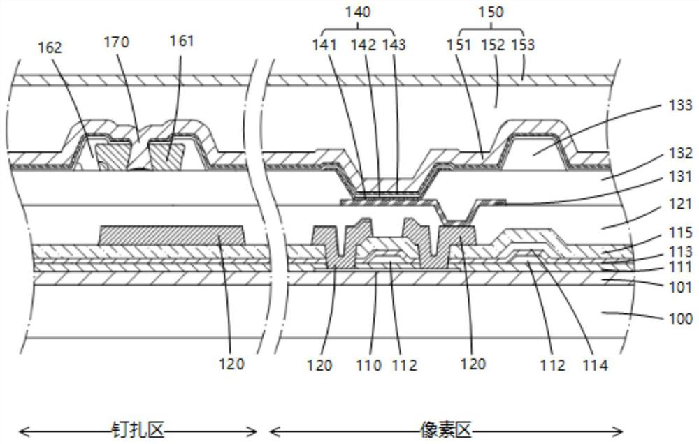
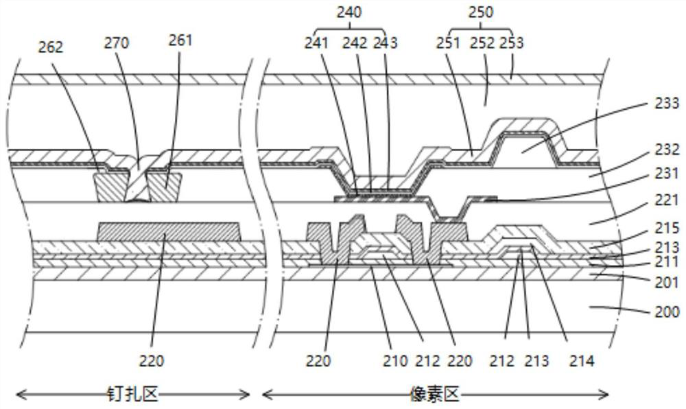
[0071]In order to illustrate the present invention more clearly, the present invention will be further described below in conjunction with the embodiments and accompanying drawings. Similar parts in the figures are denoted by the same reference numerals. Those skilled in the art should understand that the content specifically described below is illustrative rather than restrictive, and should not limit the protection scope of the present invention.

[0072] The terms "on", "formed on" and "arranged on" in the present disclosure may mean that one layer is directly formed or disposed on another layer, or that one layer is indirectly formed or disposed on another layer. Set on another layer, that is, there are other layers between the two layers.

[0073] It should be noted that although the terms "first", "second" and the like may be used herein to describe various components, components, elements, regions, layers and / or sections, these components, components, elements, regions...


PUM


Abstract

The embodiment of the invention discloses a display panel and a manufacturing method thereof. The display panel comprises a substrate; a thin film transistor layer formed on the substrate; a planarization layer formed on the thin film transistor layer; the display panel comprises a planarization layer, and is characterized in that the display panel further comprises a light-emitting element and a pinning structure which are formed on the planarization layer, the light-emitting element and the pinning structure are located in a pixel area and a pinning area of the display panel respectively, and the pinning structure comprises a groove; and the packaging layer covers the light-emitting element and the pinning structure, and at least partial area of the packaging layer is embedded in the groove.

Description

technical field [0001] The invention relates to the field of display technology. More specifically, it relates to a display panel and a manufacturing method thereof. Background technique [0002] With the development of display technology, flexible display devices have appeared in the market for folding screens. Compared with traditional display devices, folding screens have significant advantages. Peeling, shedding problem. An important reason for the current failure is that the adhesion between the layers of the organic light-emitting material using the evaporation process is weak. During the repeated bending process, the long-term shear stress will cause the peeling between the layers to cause the device to fail. [0003] The Chinese patent application with the application number CN202010937199.6 discloses a display panel and its manufacturing method. An undercut structure is added to the backplane to form a pinning structure between the inorganic layer and the substrat...

Claims


Application Information

Patent Timeline
Patent Type & Authority Applications(China)
IPC IPC(8): H01L27/32H01L51/52H01L51/56G09F9/30
CPCG09F9/301H10K59/122H10K50/84H10K71/00
Inventor 张子予王涛谢春燕孙韬陈善韬
Owner BOE TECH GRP CO LTD
Why Eureka
Try Eureka