Optical waveguide device for AR (Augmented Reality) equipment, manufacturing method of optical waveguide device and AR equipment

A technology of optical waveguide and equipment, which is applied in the field of optical imaging, can solve problems such as waste, achieve the effects of reducing light energy loss, widening the field of view, and improving design freedom

Pending Publication Date: 2022-03-04
NINGBO SUNNY OPOTECH CO LTD
View PDF9 Cites 6 Cited by
  • Summary
  • Abstract
  • Description
  • Claims
  • Application Information

AI Technical Summary

Problems solved by technology

In general, more image light needs to be pointed at the user side than at the world side, as image light pointing at the world side is not only inherently wasteful, but also causes surrounding people to view user content

Method used


Image

  • Optical waveguide device for AR (Augmented Reality) equipment, manufacturing method of optical waveguide device and AR equipment
  • Optical waveguide device for AR (Augmented Reality) equipment, manufacturing method of optical waveguide device and AR equipment
  • Optical waveguide device for AR (Augmented Reality) equipment, manufacturing method of optical waveguide device and AR equipment

Examples


Embodiment Construction

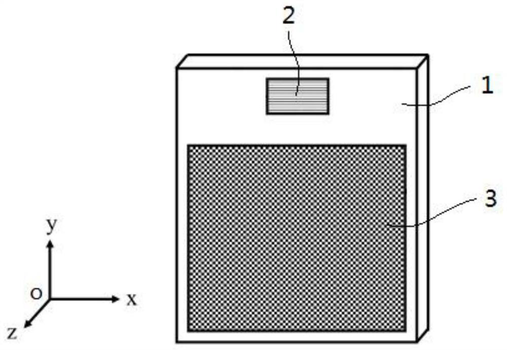
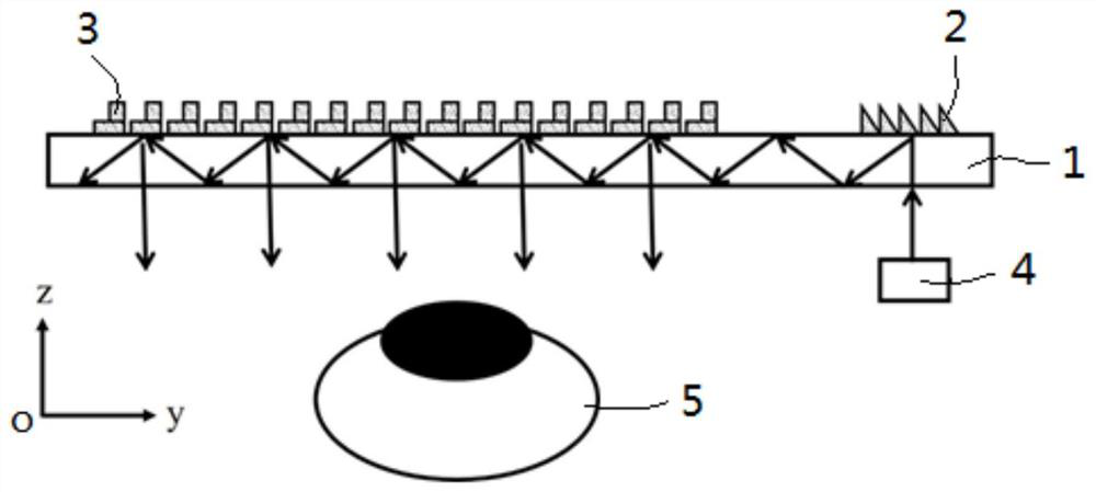
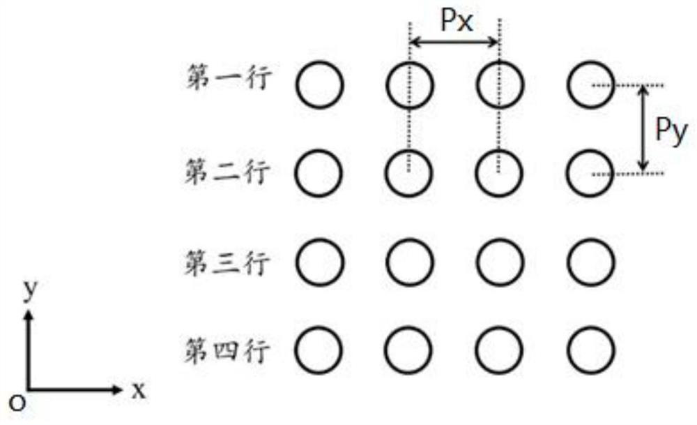
[0066] First of all, it should be noted that the optical waveguide device for AR equipment and its manufacturing method according to the present invention and the steps, construction, features and advantages of the AR equipment will be described below by way of example, but all descriptions should not be used not to impose any limitations on the present invention. In this article, the technical terms "first" and "second" are only used for the purpose of distinguishing expressions and are not intended to indicate their order and relative importance. The technical term "substantially" is intended to include The insubstantial error associated with the measurement, for example, can include the range of ±8%, ±5% or ±2% of the given value, the technical terms "upper", "lower", "right", "left", "horizontal ", "vertical" and their derivatives should be associated with the orientations in the various drawings, and it is understood that the present invention may assume many alternative ...


PUM

PropertyMeasurementUnit
thicknessaaaaaaaaaa
thicknessaaaaaaaaaa
refractive indexaaaaaaaaaa

Abstract

The invention relates to an optical waveguide device for AR equipment, a manufacturing method of the optical waveguide device and the AR equipment. The optical waveguide device comprises an optical waveguide substrate, a coupling-in area and a coupling-out area, the coupling-in area is provided with a first grating used for coupling incident light into the optical waveguide substrate, the coupling-out area is provided with a second grating used for coupling out light from the optical waveguide substrate after two-dimensional expansion, the first grating is provided with a coupling-in grating vector, and the coupling-out area is provided with a coupling-out grating vector. The second grating is provided with a first coupled-out grating vector and a second coupled-out grating vector which are crossed with each other, the grating unit arrays of the first grating and the second grating are basically parallel in one dimension direction and have the same period, and the first coupled-out grating vector and the second coupled-out grating vector are symmetrical relative to the coupled-in grating vector; the second grating is a two-dimensional surface relief grating and is of a three-order cylinder array structure. The invention has the advantages of simple and compact structure, large field angle range, small light energy loss, strong equipment cruising ability and the like.

Description

technical field [0001] The invention relates to the technical field of optical imaging, in particular to an optical waveguide device for AR equipment, a manufacturing method thereof, and the AR equipment. Background technique [0002] The optical waveguide is the key core component in the new generation of augmented reality technology (Augmented Reality, AR). It combines the principle of total reflection waveguide and diffraction elements to replicate the extended exit pupil in the imaging system. Due to its large pupil , small size, light weight and other advantages, it has become an inevitable trend in the development of AR technology. [0003] Typical optical waveguide technology is to project the image light source emitted by the microdisplay into the incident grating area of ​​the optical waveguide sheet through the projection lens, which is captured by the optical waveguide sheet and transmitted to the second grating area by total reflection and then deflected by 90° b...

Claims


Application Information

Patent Timeline
Patent Type & Authority Applications(China)
IPC IPC(8): G02B6/00G02B6/10G02B5/18G02B27/01
CPCG02B6/10G02B6/0033G02B5/1814G02B27/0101G02B5/18G02B27/01G02B6/00G02B6/124
Inventor 徐钦锋马珂奇杜佳玮
Owner NINGBO SUNNY OPOTECH CO LTD
Why Eureka
Try Eureka