Circuit board with buffer layer and heat conduction admixtures

A buffer layer, circuit board technology, applied in circuit thermal devices, printed circuit components, printed circuit stress/deformation reduction, etc., can solve problems such as poor reliability

Pending Publication Date: 2022-03-08
BRIDGE SEMICON
View PDF3 Cites 0 Cited by
  • Summary
  • Abstract
  • Description
  • Claims
  • Application Information

AI Technical Summary

Problems solved by technology

However, due to the low CTE (coefficient of thermal expansion) of the ceramic material, it is easy to generate extreme stress due

Method used


Image

  • Circuit board with buffer layer and heat conduction admixtures
  • Circuit board with buffer layer and heat conduction admixtures
  • Circuit board with buffer layer and heat conduction admixtures

Examples


no. 1 example

[0020] Figure 1-5 In the first embodiment of the present invention, a diagram of a manufacturing method of a circuit board includes an interconnect base, a thermoelectric conductor, a bonding layer, a top buffer layer, a thermally conductive additive, and a top routing layer.

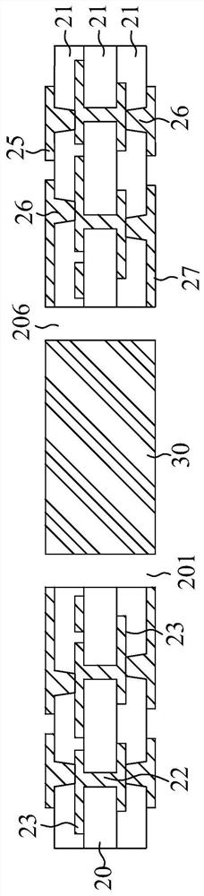
[0021] figure 1 It is a sectional view of inserting the thermoelectric conductor 30 into the opening 201 of the interconnection base 20 . The opening 201 of the interconnect base 20 extends from the top surface to the bottom surface, which can be formed by various techniques, such as punching, drilling or laser cutting. The inner sidewall of the opening 201 of the interconnect base 20 laterally surrounds the peripheral sidewall of the thermoelectric conductor 30 and is spaced apart from the peripheral sidewall of the thermoelectric conductor 30 . Therefore, the gap 206 is located in the opening 201 between the inner sidewall of the interconnection base 20 and the peripheral sidewall of the thermoelec...

no. 2 example

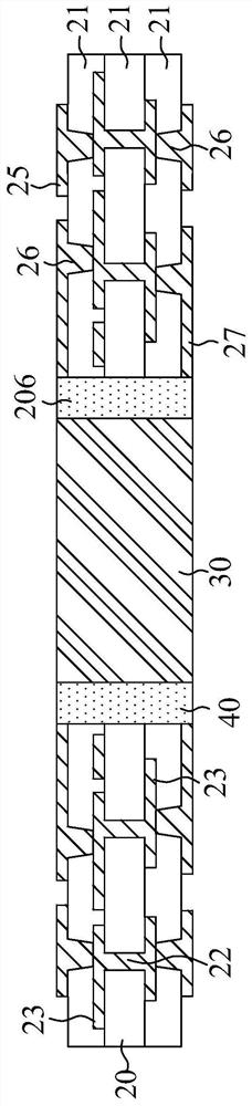
[0029] Figure 6 It is a sectional view of the circuit board of the second embodiment of the present invention.

[0030] For the purpose of brief description, any descriptions in the above first embodiment that can be used in the same way are incorporated here, and the same descriptions do not need to be repeated.

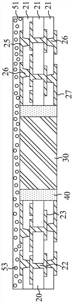
[0031] The circuit board 200 is similar to Figure 5 The structure shown is different in that the top buffer layer 51 further contains a reinforcing admixture 55 , which is mixed with the thermally conductive admixture 53 in the top buffer layer 51 to improve the reliability of the top buffer layer 51 . More specifically, the reinforcing admixture 55 is preferably a fibrous inorganic material with a higher elastic modulus than the top buffer layer 51, for example, the elastic modulus of the reinforcing admixture 55 may be higher than the elastic modulus of the top buffer layer 51 At least about 10 GPa. Accordingly, the combination of the top cushioning layer 51 ...

no. 3 example

[0033] Figure 7 It is a sectional view of the circuit board of the third embodiment of the present invention.

[0034] For the purpose of brief description, any descriptions in the above-mentioned first embodiment and second embodiment that can be used in the same way are incorporated here, and it is not necessary to repeat the same descriptions.

[0035] The circuit board 300 is similar to Figure 5 The structure shown is different in that it further includes a bottom buffer layer 52 and a bottom routing layer 62 . The bottom buffer layer 52 laterally extends from the bottom surface of the thermoelectric conductor 30 to the bottom surface of the interconnection base 20 to cover the interconnection base 20 , the thermoelectric conductor 30 and the bonding layer 40 from below. Similar to the top buffer layer 51, the elastic modulus of the bottom buffer layer 52 is lower than the elastic modulus of the thermoelectric conductor 30, for example, the elastic modulus of the botto...


PUM

PropertyMeasurementUnit
Thermal expansion coefficientaaaaaaaaaa
Thermal conductivityaaaaaaaaaa
Modulusaaaaaaaaaa

Abstract

The circuit board mainly comprises an interconnection base, a thermoelectric conductor, a joint layer, a top buffer layer, at least one heat conduction adulteration and a top routing layer. An interconnect base is attached around the peripheral sidewall of the thermoelectric conductor by a bonding layer, and a top buffer layer mixed with a thermally conductive admixture overlies the thermoelectric conductor and the interconnect base and is located between the top routing layer and the interconnect base/thermoelectric conductor. The top buffer layer has an elastic modulus smaller than that of the thermoelectric conductor, so that a stress buffer effect can be provided. The thermally conductive admixtures dispersed in the top buffer layer facilitate conduction of heat generated by a device assembled on the top routing layer from the top routing layer to the thermoelectric conductor. Therefore, the circuit board provided by the invention can show excellent thermoelectric efficiency and reliability.

Description

technical field [0001] The invention relates to a circuit board, especially a circuit board with a buffer layer and a heat-conducting admixture. Background technique [0002] High-performance microprocessors and ASICs require high-performance circuit boards to interconnect signals. However, as the power increases, the large amount of heat generated by the semiconductor chip will degrade the performance of the device and cause thermal stress on the chip. Therefore, it is critical to choose an insulating substrate with better heat dissipation efficiency. Ceramic materials (such as alumina or aluminum nitride) have been widely used as substrate materials due to their ideal electrical insulation, high mechanical strength, and good thermal conductivity. Although ceramic materials have both thermal conductivity and electrical insulation properties, they still cannot meet the required heat dissipation requirements in some applications, and the metallization technology, wiring tech...

Claims


Application Information

Patent Timeline
IPC IPC(8): H05K1/02
CPCH05K1/0201H05K1/0271
Inventor 林文强王家忠
Owner BRIDGE SEMICON
Why Eureka
Try Eureka