Etching device for manufacturing integrated optoelectronic device

A technology for optoelectronic devices and etching devices, which is applied in semiconductor/solid-state device manufacturing, electrical components, and final product manufacturing, etc. It can solve problems that affect the etching effect of integrated optoelectronic devices, uneven etching of integrated optoelectronic devices, and failure to meet user needs. , to achieve the effect of improving the etching effect, improving the practical performance and improving the use effect

Active Publication Date: 2022-03-11
GUILIN TRYIN TECH CO LTD
View PDF4 Cites 4 Cited by
  • Summary
  • Abstract
  • Description
  • Claims
  • Application Information

AI Technical Summary

Problems solved by technology

[0003] Nowadays, with the rapid development of electronic technology, integrated optoelectronic devices are made more and more finely. In the production process of integrated optoelectronic devices, the etching process is particularly important, and the existing etching devices are used to etch electronic devices. In the process, there will be the following problems. One: the traditional etching technology is mainly carried out manually, but this method cannot ensure that the etchant on the surface of the integrated optoelectronic device is uniformly applied, resulting in uneven etching of the integrated optoelectronic device. Less than the ideal effect; second: when the etching solution is applied to the surface of the integrated optoelectronic device, the etching equipment is prone to shake, which in turn affects the etching effect of the integrated optoelectronic device; therefore, there are deficiencies and cannot meet the needs of users. Therefore, There is a need for further improvement

Method used


Image

  • Etching device for manufacturing integrated optoelectronic device
  • Etching device for manufacturing integrated optoelectronic device
  • Etching device for manufacturing integrated optoelectronic device

Examples


Embodiment Construction

[0030] The following will clearly and completely describe the technical solutions in the embodiments of the present invention in conjunction with the accompanying drawings in the embodiments of the present invention. Obviously, the described embodiments are only some embodiments of the present invention, not all embodiments, and It should be noted that, in the case of no conflict, the embodiments in the present invention and the features in the embodiments can be combined with each other. "The word only means that it is consistent with the upper, lower, left and right directions of the drawing itself, and does not limit the structure. Based on the embodiments of the present invention, those of ordinary skill in the art have obtained it without creative work. All other embodiments of all belong to the protection scope of the present invention.

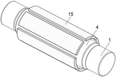
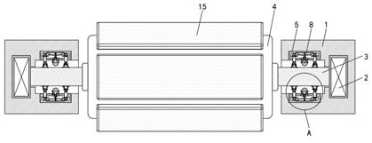
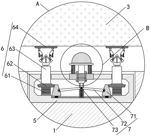
[0031] see Figure 1 to Figure 7, an etching device for the manufacture of integrated optoelectronic devices, comprising a main body ...


PUM


Abstract

The invention provides an etching device for manufacturing an integrated optoelectronic device, which comprises a main body, a driving mechanism is arranged in the main body, a driving shaft is arranged on the driving mechanism, an etching device is arranged on the driving shaft, a fixing component is arranged on the inner wall of the main body, and the fixing component is arranged on the inner wall of the main body. An offset sensing assembly, a linkage assembly and a correction assembly are arranged on the fixing part; the deviation induction assembly comprises an induction air cushion, a movable part, an induction main rod and a guide part. According to the etching device for manufacturing the integrated optoelectronic device, by arranging the correction assembly, once the etching device shakes, the etching device inevitably drives the driving shaft to synchronously shake, and the correction main rod is utilized to drive the correction piece to be in contact with the driving shaft, so that the driving shaft which deviates due to shaking is corrected; therefore, the problem of jittering of the etching device is fundamentally solved, the etching effect of the etching device on the integrated optoelectronic device is improved, and meanwhile, the reliability of the equipment is effectively improved.

Description

technical field [0001] The invention belongs to the technical field of electronic device manufacturing, and in particular relates to an etching device for manufacturing integrated optoelectronic devices. Background technique [0002] The basic process of the production of integrated optoelectronic devices generally includes the development process, etching process and film removal process. The development process refers to the use of developer to dissolve the part of the film that has not been irradiated by ultraviolet rays, and retain the part that has undergone polymerization reaction after ultraviolet radiation; the etching process It refers to the use of etching solution to etch away the exposed copper on the integrated optoelectronic device that is not protected by the protective film; the film removal process refers to removing the protective film on the integrated optoelectronic device to expose the processed circuit. [0003] Nowadays, with the rapid development of e...

Claims


Application Information

Patent Timeline
Patent Type & Authority Applications(China)
IPC IPC(8): H01L21/67H01L21/306C23F1/02C23F1/08
CPCH01L21/67075H01L21/67259H01L21/30604C23F1/08C23F1/02Y02P70/50
Inventor 王垚磊张见超王建国
Owner GUILIN TRYIN TECH CO LTD
Why Eureka
Try Eureka