A low power consumption and high precision protocol integrated circuit module packaging process

A technology of integrated circuit and packaging technology, which is applied in the field of low power consumption and high-precision protocol integrated circuit module packaging technology, which can solve the problems of expanding the defective rate of product packaging production, the flying line is vulnerable to flow impact, chip offset and other problems, and achieves the reduction Probability of product breaking under force, improving production stability, and ensuring the effect of stable packaging

Active Publication Date: 2022-04-19
江苏高格芯微电子有限公司
View PDF3 Cites 0 Cited by
  • Summary
  • Abstract
  • Description
  • Claims
  • Application Information

AI Technical Summary

Problems solved by technology

[0003] When the circuit module is produced, in order to ensure its stability in the later installation and use process, it needs to be packaged. The circuit module packaging process in the prior art is mostly directly on the top of the circuit substrate after the chip is installed. Carry out the plastic encapsulation operation, and directly encapsulate the chips and other units in the epoxy resin. Although this method can effectively implement the encapsulation operation on the circuit substrate, in the actual encapsulation process, it is affected by the flow of the epoxy resin injection process, resulting in the circuit The chips on the substrate and the flying leads of the chips are easily impacted by the flow, causing the chips to shift, the flying leads to break, and the wires to be merged, thereby expanding the defect rate of the product packaging production to a certain extent.

Method used


Image

  • A low power consumption and high precision protocol integrated circuit module packaging process
  • A low power consumption and high precision protocol integrated circuit module packaging process
  • A low power consumption and high precision protocol integrated circuit module packaging process

Examples


Embodiment 1

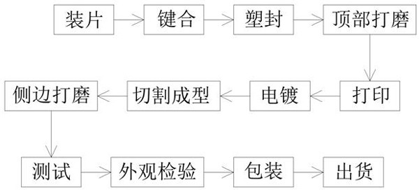
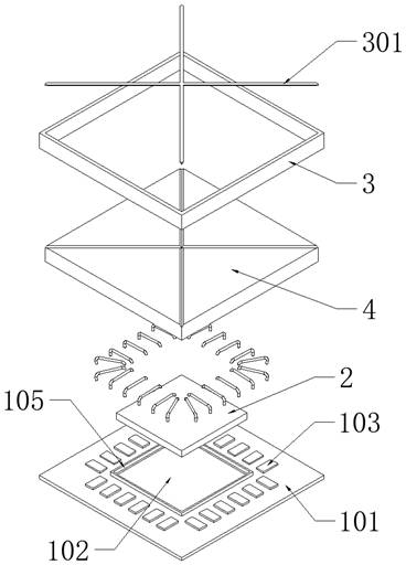
[0057] see Figure 1-Figure 10 , a low-power-consumption high-precision protocol integrated circuit module packaging process, comprising the following steps:

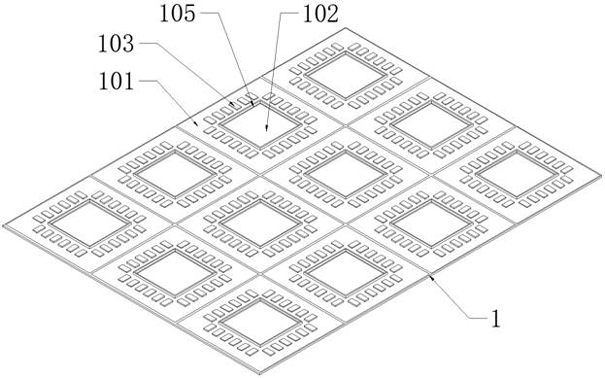
[0058] S1. Chip loading: The interior of the main board 1 is evenly divided into a plurality of circuit substrates 101, and each circuit substrate 101 is provided with a mounting position 102 in the middle of the top, and a plurality of inlaid circuit boards are arranged around the mounting position 102. The first contact 103 on the top of the substrate 101, and the second contact 104 corresponding to the plurality of first contacts 103 are evenly inlaid on the bottom of the circuit substrate 101, and the chip 2 is sequentially placed on the installation position set on the top of the circuit substrate 101 by the grasping robot arm 102 on;

[0059] S2. Bonding: use the welding manipulator to connect the connection point on the chip 2 and the contact point 103 with flying wires. After the flying wire operation is comple...


PUM


Abstract

The invention discloses a low-power consumption and high-precision protocol integrated circuit module packaging process, which can reduce the probability of chip offset, flying wire breakage or parallel connection between flying wires during the packaging process of the circuit module. When bonding, the metal frame is fixedly set on the top of the circuit substrate, and the reinforcing rib is fixedly installed on the top of the metal frame, which can effectively reduce the probability of chips and flying leads being affected by the flow of epoxy resin during injection molding packaging, which is conducive to improving Production stability. At the same time, by installing the metal frame on the top of the circuit substrate, the probability of product fracture during later cutting can be reduced, which is conducive to improving the structural strength of the small circuit module produced by this process. To a certain extent Improved product quality.

Description

technical field [0001] The invention relates to the field of circuit module packaging, and more specifically relates to a low-power consumption and high-precision protocol integrated circuit module packaging process. Background technique [0002] Nowadays, the main trend of products in the global fast charging protocol market is high efficiency and high reliability. Among them, the charging protocol fast charging 3.0 is based on a chip (2) mV increment, which can provide mobile phones with flexible voltage from 3.6V to 12V. Selection, so that the mobile phone can obtain just the right voltage, so as to achieve the expected charging current, can achieve the effect of minimizing power loss, improving charging efficiency and improving thermal performance, and is widely loaded in today's circuit modules. [0003] When the circuit module is produced, in order to ensure its stability in the later installation and use process, it needs to be packaged. The circuit module packaging p...

Claims


Application Information

Patent Timeline
Patent Type & Authority Patents(China)
IPC IPC(8): H01L21/60H01L21/56H01L21/68H01L23/373H01L23/367
CPCH01L24/81H01L21/56H01L21/68H01L23/3737H01L23/3736H01L23/367H01L2224/81007
Inventor 魏永红魏霄鸿马吉祥王国霖李星星
Owner 江苏高格芯微电子有限公司
Why Eureka
Try Eureka