A high-precision integrated circuit chip packaging device and its packaging process

An integrated circuit and chip packaging technology, applied in circuits, electrical components, electrical solid devices, etc., can solve the problems of low chip bonding stability, increased manufacturing costs, no seismic performance and high heat dissipation, etc. The effect of light curing efficiency, improving packaging efficiency and shortening light curing time

Active Publication Date: 2022-04-19
江苏高格芯微电子有限公司
View PDF4 Cites 0 Cited by
  • Summary
  • Abstract
  • Description
  • Claims
  • Application Information

AI Technical Summary

Problems solved by technology

However, in the actual packaging process, especially in the packaging process of high-precision integrated circuit chips, due to the low stability of chip bonding, it is easy to cause chip peeling and dislocation during the process of packaging with resin, which will affect the semiconductor stack. The stability of the packaging structure leads to an increase in manufacturing costs. At the same time, the existing packaging devices do not have shock resistance and high heat dissipation, and cannot effectively protect high-precision integrated circuit chips.

Method used


Image

  • A high-precision integrated circuit chip packaging device and its packaging process
  • A high-precision integrated circuit chip packaging device and its packaging process
  • A high-precision integrated circuit chip packaging device and its packaging process

Examples


Embodiment 1

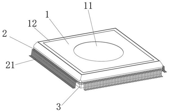
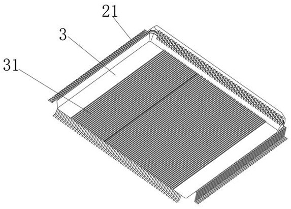
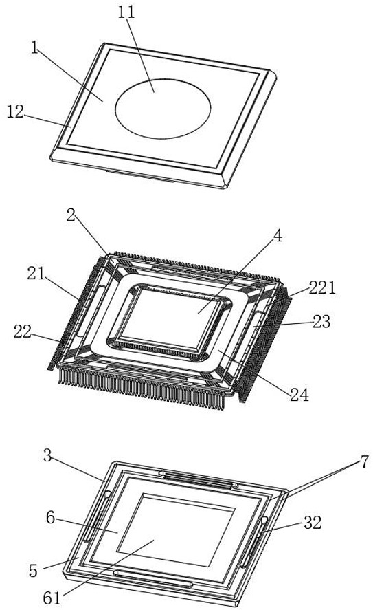
[0045] see Figure 1-Figure 10 , a high-precision integrated circuit chip packaging device, including an upper case 1, a lower case 3 and a liner 2, a chip 4 is fixed on the liner 2, and the opposite sides of the upper case 1 and the lower case 3 are A second light guide frame 5 is provided, the inside and outside of the frame of the second light guide frame 5 are provided with gluing grooves 7, and the second light guide frame 5 of the upper housing 1 is provided with a mating block 13, four mating blocks 13 The blocks 13 are equally arranged at equal angles, the top of the matching block 13 extends through the upper casing 1 and is fixed with the first light guide frame 12, and the second light guiding frame 5 of the lower casing 3 is provided with a matching The mating groove 32 that matches the block 13 is provided with an elastic capsule 14 in the mating block 13, and the elastic capsule 14 is saturated and filled with light-curing glue 9, and the bottom of the elastic ca...


PUM


Abstract

The invention discloses a high-precision integrated circuit chip packaging device and its packaging technology, comprising an upper case, a lower case and a liner, a chip is fixed on the liner, and the opposite sides of the upper case and the lower case are There is a second light guide frame, the inner and outer sides of the second light guide frame are provided with glued grooves, and the second light guide frame of the upper shell is provided with a mating block, and the four mating blocks are equiangularly divided. Arrangement, the top of the mating block extends through the upper case and is fixed with the first light guide frame, and the second light guide frame of the lower case is provided with a mating groove that matches the mating block. The structure of the present invention is simple , high packaging efficiency, strong heat dissipation and shock resistance of the packaging structure, and can be completely disassembled after packaging, easy to maintain and reuse, simple process, effectively reducing manufacturing costs, has market prospects, and is suitable for promotion.

Description

technical field [0001] The invention relates to the field of chip packaging, more specifically, to a high-precision integrated circuit chip packaging device and a packaging process thereof. Background technique [0002] In the existing semiconductor stack packaging technology, usually an adhesive material is directly arranged between the chips to complete the bonding, and then the bonded chip package is packaged with a resin material. However, in the actual packaging process, especially in the packaging process of high-precision integrated circuit chips, due to the low stability of chip bonding, it is easy to cause chip peeling and dislocation during the process of packaging with resin, which will affect the semiconductor stack. The stability of the packaging structure leads to an increase in manufacturing costs. At the same time, the existing packaging devices do not have shock resistance and high heat dissipation, and cannot effectively protect high-precision integrated ci...

Claims


Application Information

Patent Timeline
Patent Type & Authority Patents(China)
IPC IPC(8): H01L23/02H01L23/10H01L23/16H01L23/367H01L23/427F16F15/04H01L21/52
CPCH01L23/02H01L23/10H01L23/16H01L23/3672H01L23/427F16F15/04H01L21/52
Inventor 魏永红魏霄鸿马吉祥王国霖李星星
Owner 江苏高格芯微电子有限公司
Why Eureka
Try Eureka