

Flip-chip light emitting diode and light emitting device
A light-emitting diode and flip-chip technology, which is applied in the direction of electrical components, circuits, semiconductor devices, etc., can solve problems such as easy puncture of thimbles, influence on the reliability of flip-chip light-emitting diodes, leakage failure of flip-chip light-emitting diodes, etc., and achieve risk reduction Effect
- Summary
- Abstract
- Description
- Claims
- Application Information
AI Technical Summary
Problems solved by technology
Method used
Image


Examples
Embodiment 1
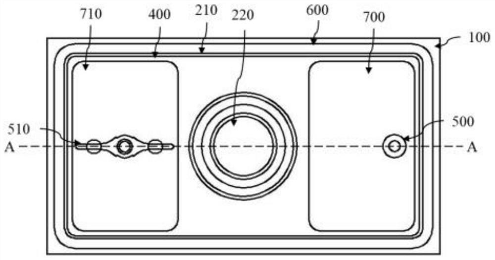
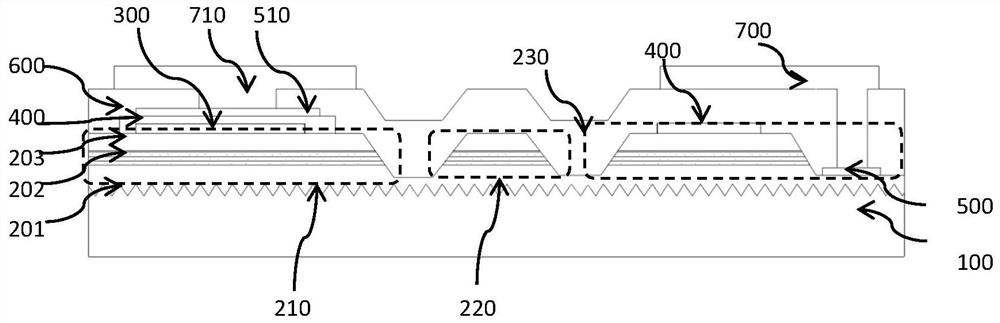
[0073] According to one aspect of the present application, a flip-chip light emitting diode is provided. Figure 1a , 2a is the top view of the flip-chip light-emitting diode, Figure 1b , 2b , 3-4 for Figure 1a , 2a A-A cross-sectional schematic diagram.
[0074] The flip-chip light emitting diode includes a substrate and a semiconductor stack layer on the substrate; the semiconductor stack layer includes an island structure and at least one semiconductor light emitting unit, and the groove is located between the semiconductor light emitting unit and the island structure.
[0075] The flip-chip light emitting diode includes a substrate 100 and a semiconductor stack layer on the substrate, and the semiconductor stack layer includes a first semiconductor layer 201 , an active layer 202 and a second semiconductor layer 203 . The semiconductor stack layer includes an island structure 220 and a semiconductor light emitting unit 210, the semiconductor light emitting unit 210 su...
Embodiment 2
[0105] High-voltage flip-chip light-emitting diodes, as a modified design of conventional flip-chip light-emitting diodes, are divided into multiple sub-semiconductor light-emitting units with equal areas by trenches, and then the sub-semiconductor light-emitting units are electrically connected in series / parallel with each other. This design leads to grooves in the central area of the even-numbered sub-semiconductor light-emitting units. When flip-chip LEDs are transferred, thimbles need to be used to act on the middle area of one side of the front electrode of the LEDs. When the grooves are located in the central area, the insulating layer due to The unevenness is easy to be cracked by the thimble, causing water vapor to easily invade the interior of the self-luminous unit along the cracked position, and the light-emitting diode is prone to failure during aging tests or long-term use.
[0106] Aiming at this problem, the present invention designs a high-voltage flip-chip ...
Embodiment 3
[0132] The present application provides a method for preparing a flip-chip light-emitting diode, and specifically provides a method for preparing a flip-chip light-emitting diode as shown in FIG. 1 . The preparation method comprises the following steps:
[0133] S1, see Figure 10 , providing a substrate 100 , and forming a semiconductor stack layer 200 on the substrate 100 .
[0134] The semiconductor stack 200 includes a first semiconductor layer 201, an active layer 202 and a second semiconductor layer 203; the first semiconductor layer 201 is an N-type semiconductor layer, the active layer 202 is a multilayer quantum well layer, and the second semiconductor layer 203 is P-type semiconductor layer. In this embodiment, the substrate 100 is a patterned sapphire substrate or a flat sapphire substrate.
[0135] S2, see Figure 11 , etch the semiconductor stack layer 200 and form a groove 230 through the semiconductor stack layer 200, the groove 230 is annular and divides th...
PUM
| Property | Measurement | Unit |
|---|---|---|
| thickness | aaaaa | aaaaa |
| width | aaaaa | aaaaa |
| thickness | aaaaa | aaaaa |
Abstract
Description
Claims
Application Information