

PCB wiring method for compensating signal delay, PCB and electronic equipment
A kind of PCB board, compensation signal technology, applied in CAD circuit design, electrical digital data processing, computer-aided design and other directions, can solve the problems of large PCB board space, inability to perform delay compensation, insufficient winding space, etc., to save The effect of taking up space, shortening the length of the winding, and meeting the timing requirements
- Summary
- Abstract
- Description
- Claims
- Application Information
AI Technical Summary
Problems solved by technology
Method used
Image

Examples
Embodiment 1
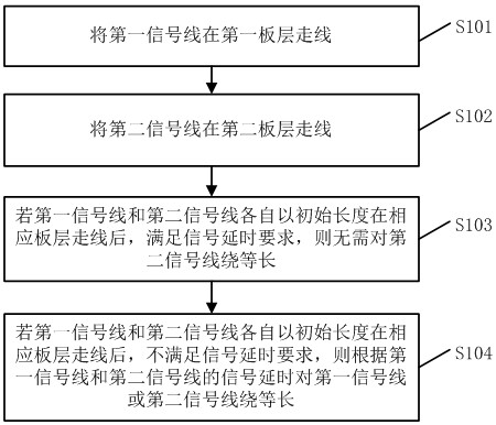
[0041] Such as figure 2 Shown is a schematic flow chart of a PCB routing method for compensating signal delay provided in the first embodiment, and the method includes the following steps.
[0042] S101, route the first signal line on the first board layer.
[0043] S102 , route the second signal line on the second board layer.
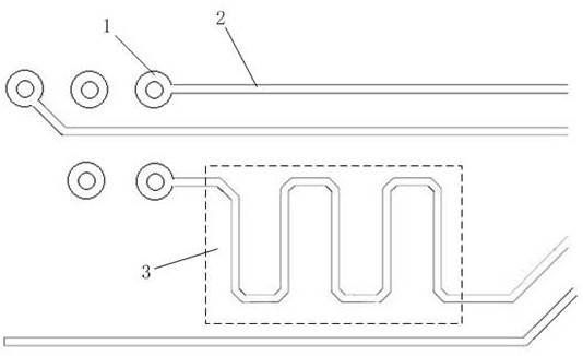
[0044] S103, if the first signal line and the second signal line are respectively routed on corresponding board layers with initial lengths and meet the signal delay requirement, there is no need to wind the second signal lines to equal lengths.
[0045] S104, if the first signal line and the second signal line are respectively routed on the corresponding board layer with the initial length and do not meet the signal delay requirement, then adjust the first signal line according to the signal delay of the first signal line and the second signal line wire or the second signal wire is wound with equal length.
[0046] Wherein, the unit length delay ...
Embodiment 2
[0083] The second embodiment provides a PCB board, which uses the wiring method of the first embodiment above for wiring.
Embodiment 3
[0085] The third embodiment provides an electronic device, including the PCB board of the second embodiment.
PUM
 Abstract
Description
Claims
Application Information