

Multilayer step PCB manufacturing method, PCB and electronic equipment
A technology of PCB board and manufacturing method, which is applied in the direction of removing conductive materials, printed circuits, electrical components, etc. by chemical/electrolytic methods, and can solve problems such as low reliability, many times of pressing, and high cost, so as to avoid steps. The effect of glue flow, good reliability and short process
- Summary
- Abstract
- Description
- Claims
- Application Information
AI Technical Summary
Problems solved by technology
Method used
Image

Examples
Embodiment 1
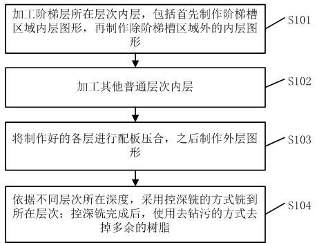
[0031] Such as figure 1 Shown is a schematic flow chart of a method for manufacturing a multi-level ladder PCB provided in Embodiment 1, including the following steps.
[0032] S101. Processing the inner layer of the layer where the step layer is located includes first making the inner layer graphics in the stepped groove area, and then making the inner layer graphics except the stepped groove area.
[0033] Firstly, the inner layer of the layer where the step layer is located is processed. The layer where the step layer is located includes the step groove area and the non-step groove area. These two types of areas use different processes to make the inner layer graphics, so they should be produced separately. Specifically, the inner layer graphics in the stepped groove area are made first, and then the inner layer graphics except the stepped groove area are made.
[0034] S102, processing other common layer inner layers.
[0035] In S103, the prepared layers are matched and...
Embodiment 2
[0041] This embodiment 2 provides a method for manufacturing a multi-layer ladder PCB board. First, process the inner layer of the layer where the ladder layer is located, including first making the inner layer graphics in the stepped groove area, and then making the inner layer graphics except the stepped groove area; and then processing other common For the inner layer of the layer, the prepared layers are matched and pressed together, and then the outer layer graphics are made, and then according to the depth of different layers, milling is carried out to the corresponding layer by means of controlled depth milling; after the controlled depth milling is completed, use the drill to remove dirt way to remove excess resin. Wherein, when processing the inner layer of the layer where the stepped layer is located, the inner layer graphics in the stepped groove area are firstly made, and then the inner layer graphics except the stepped groove area are made. Among them, different p...
Embodiment 3
[0060] In the method for manufacturing a multi-layered stepped PCB board provided in Embodiment 3, firstly process the inner layer of the layer where the stepped layer is located, including first making the inner layer graphics in the stepped groove area, and then making the inner layer graphics except the stepped groove area; and then processing other For the inner layer of the ordinary layer, the prepared layers are matched and pressed together, and then the outer layer graphics are made, and then according to the depth of different layers, the method of controlled depth milling is used to mill to the corresponding layer; after the controlled depth milling is completed, use de-drilling Remove excess resin in a dirty manner.
[0061] Wherein, when processing the inner layer of the layer where the stepped layer is located, the inner layer graphics in the stepped groove area are firstly made, and then the inner layer graphics except the stepped groove area are made. Among them,...
PUM
 Abstract
Description
Claims
Application Information