Method for rapidly detecting internal microstructure of nano electronic device based on F-SRU network

A technology of electronic devices and detection methods, which is applied in the field of rapid detection of internal microstructures of nanoelectronic devices based on F-SRU network, can solve the problems of damaged devices, reduced detection reliability, complicated measurement process, etc., so as to reduce adverse effects and improve Optimizing ability and ensuring the effect of reliability

Active Publication Date: 2022-04-08
昆山毅普腾自动化技术有限公司
View PDF8 Cites 0 Cited by
  • Summary
  • Abstract
  • Description
  • Claims
  • Application Information

AI Technical Summary

Problems solved by technology

But its disadvantages are: 1) the transmitted electron beam will damage the device; 2) the charging phenomenon generated under the electron beam irradiation will reduce the reliability of the detection; 3) the surface of the device needs to be coated with gold during the detection process, and the measurement process is more complicated ; The measurement environment is demanding, and the process detection cannot be quickly realized, and it is not practical for engineering
However, due to the complexity of model construction, there are no research progress and reports on the application of deep learning methods in the detection of the internal microstructure of nanoelectronic devices.

Method used


Image

  • Method for rapidly detecting internal microstructure of nano electronic device based on F-SRU network
  • Method for rapidly detecting internal microstructure of nano electronic device based on F-SRU network
  • Method for rapidly detecting internal microstructure of nano electronic device based on F-SRU network

Examples


Embodiment Construction

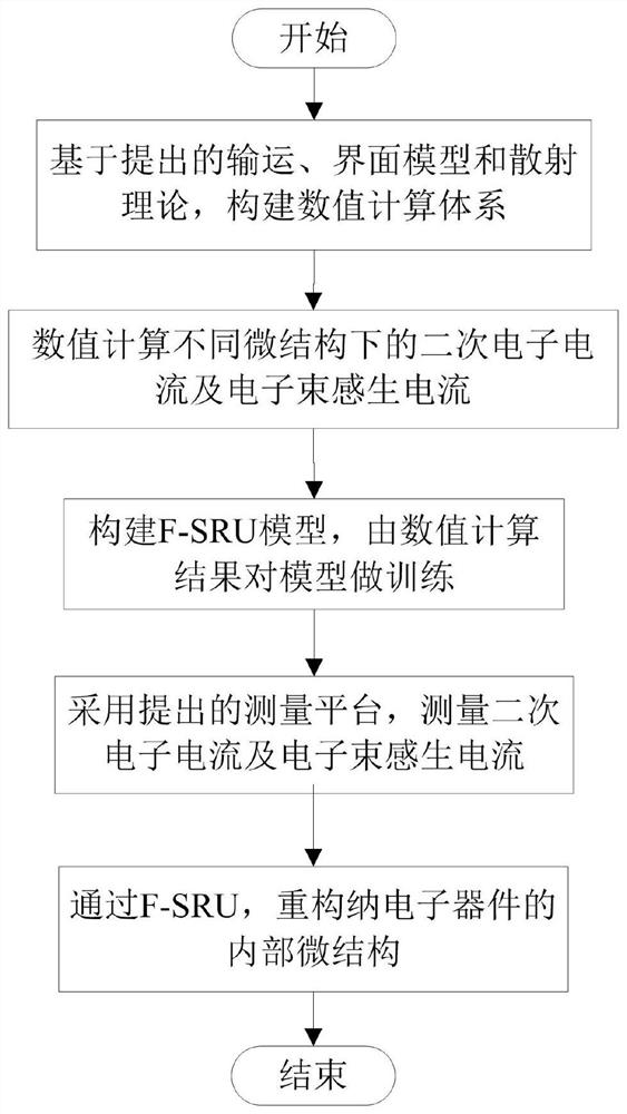
[0084] In order to make the purpose, technical solutions and advantages of the embodiments of the present invention clearer, the technical solutions in the embodiments of the present invention will be clearly and completely described below in conjunction with the drawings in the embodiments of the present invention. Obviously, the described embodiments It is a part of embodiments of the present invention, but not all embodiments. The components of the embodiments of the invention generally described and illustrated in the figures herein may be arranged and designed in a variety of different configurations.

[0085] Accordingly, the following detailed description of the embodiments of the invention provided in the accompanying drawings is not intended to limit the scope of the claimed invention, but merely represents selected embodiments of the invention. Based on the embodiments of the present invention, all other embodiments obtained by persons of ordinary skill in the art wi...


PUM


Abstract

The invention discloses an F-SRU network-based nano electronic device internal microstructure rapid detection method, which comprises the following steps: step 1, aiming at various nano electronic devices, under given electron beam working conditions and physical parameter conditions, obtaining secondary electron currents and electron beam induced currents corresponding to different microstructures by adopting numerical calculation, forming a data set of secondary electron current and electron beam induced current; step 2, constructing an F-SRU network model, and establishing a corresponding relation between an internal microstructure of the device and a related current according to a data set of a secondary electron current and an electron beam induced current obtained through calculation; 3, building a measurement platform, and rapidly measuring the secondary electron current and the electron beam induced current of the detected object; and 4, taking the measurement results of the secondary electron current and the electron beam induced current as the input of the F-SRU model, and reconstructing the internal microstructure through the output of the model.

Description

technical field [0001] The invention belongs to the technical field of nanoelectronic device detection, and in particular relates to a fast detection method for internal microstructures of nanoelectronic devices based on an F-SRU network. Background technique [0002] The development of modern nanoscale electronic technology puts forward extremely high requirements for its manufacturing process. In order to ensure the yield rate of the product, it is necessary to conduct process inspection on the semi-finished and finished products of the device. Among them, the micro-scale structural information such as the trench structure and interface structure inside the device is the key factor affecting the performance of the device, and it is also the main content of the device process inspection. [0003] However, traditional detection methods such as X-ray technology, ultrasonic technology, optical microscopy technology, etc. can only realize the structural detection of micron-sca...

Claims


Application Information

Patent Timeline
Patent Type & Authority Applications(China)
IPC IPC(8): G01R31/00G01N23/00B81C99/00G06N3/08
Inventor 张军
Owner 昆山毅普腾自动化技术有限公司
Why Eureka
Try Eureka