SONOS memory and preparation method thereof

A memory and shallow trench isolation technology, applied in the field of SONOS memory and its preparation, can solve the problem of small voltage threshold of SONOS memory, and achieve the effect of increasing the effective contact area and increasing the voltage threshold

Pending Publication Date: 2022-04-08
SHANGHAI HUALI MICROELECTRONICS CORP
View PDF0 Cites 0 Cited by
  • Summary
  • Abstract
  • Description
  • Claims
  • Application Information

AI Technical Summary

Problems solved by technology

[0003] SONOS memory realizes the tunneling of charges from the drain region to the silicon nitride layer by applying a voltage between the storage gate and the drain, and is trapped by traps in the silicon nitride layer. The ability of SONOS memory to store charges is the threshold voltage It is closely related to the characteristics of the ONO film in the storage gate and the effective area between the ONO film and the active area of ​​the substrate, but the process of the ONO film in the existing process is relatively stable, and the voltage threshold of the SONOS memory is small

Method used


Image

  • SONOS memory and preparation method thereof
  • SONOS memory and preparation method thereof
  • SONOS memory and preparation method thereof

Examples


Embodiment 1

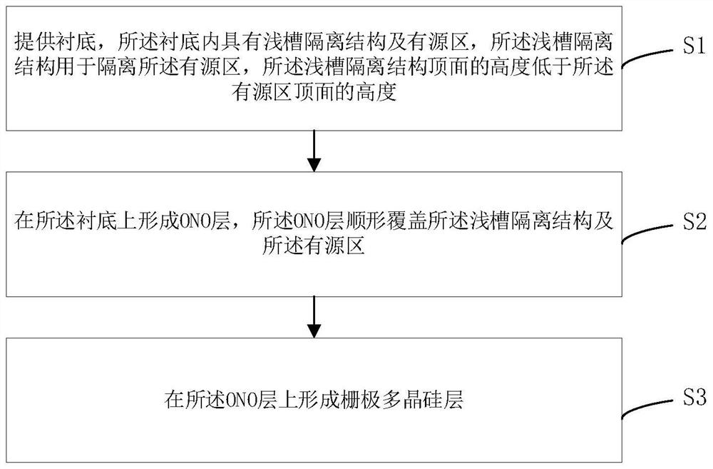
[0041] image 3 A flow chart of a method for preparing a SONOS memory provided in this embodiment, such as image 3 As shown, the invention provides a kind of preparation method of SONOS memory structure, comprising:

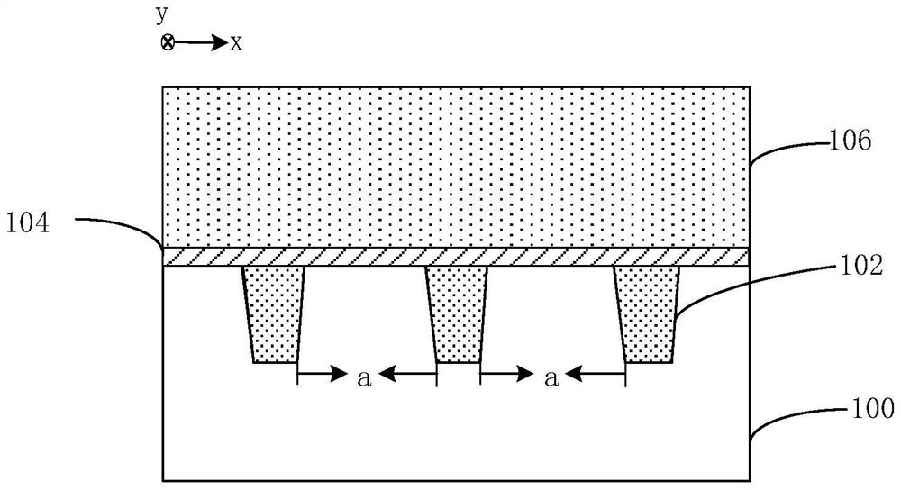
[0042] Step S1: providing a substrate, the substrate has a shallow trench isolation structure and an active region, the shallow trench isolation structure is used to isolate the active region, and the height of the top surface of the shallow trench isolation structure is lower than the height of the shallow trench isolation structure The height of the top surface of the active region;

[0043] Step S2: forming an ONO layer on the substrate, the ONO layer conformally covering the shallow trench isolation structure and the active region;

[0044] Step S3: forming a gate polysilicon layer on the ONO layer.

[0045] Figure 4a~4d A schematic structural diagram corresponding to the corresponding steps of the preparation method of a SONOS memory provided in this e...

Embodiment 2

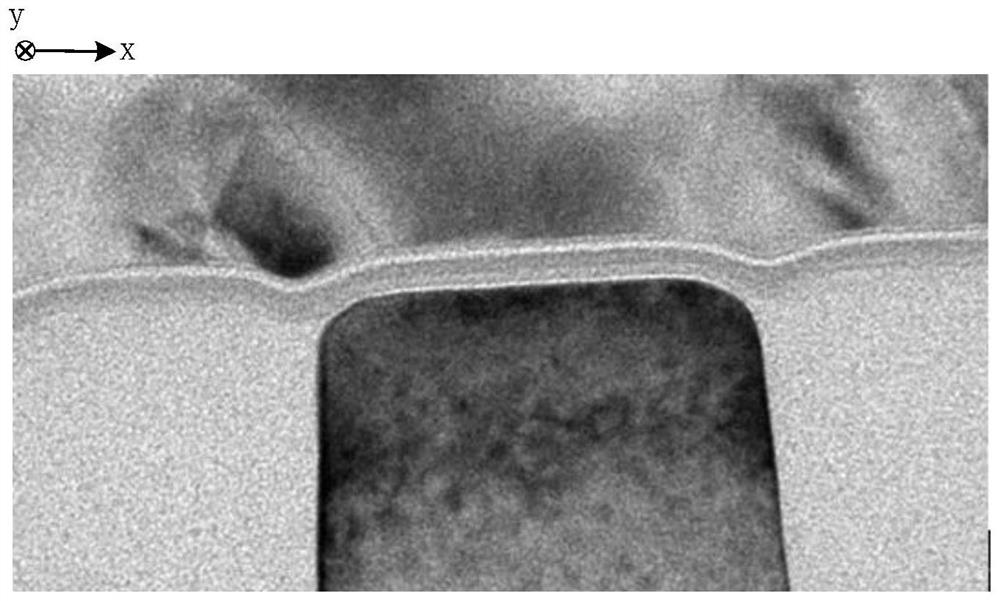
[0057] Figure 7a~7b A schematic structural view of a method for preparing a SONOS memory provided in this embodiment, as Figure 7a As shown, the difference from Embodiment 1 is that in this embodiment, after the shallow trench isolation structure 202 is etched, the active region A is also etched, so that the top surface of the active region A is Wavy, sawtooth, or square.

[0058] For example, in this embodiment, the top surface of the active region A is zigzag, and in other optional embodiments, the top surface of the active region A can also be wave-shaped or square-shaped, etc. . Changing the shape of the top surface of the active region A is to increase the area of ​​the top surface of the active region A, thereby increasing the effective contact area between the ONO layer 204 and the active region A, and increasing the SONOS memory voltage threshold.

[0059] Wherein, the active region A may be etched by a wet etching process or a dry etching process.


PUM

PropertyMeasurementUnit
thicknessaaaaaaaaaa

Abstract

According to the SONOS memory and the preparation method thereof provided by the invention, the SONOS memory comprises a substrate, a shallow trench isolation structure and an active region are arranged in the substrate, the shallow trench isolation structure is used for isolating the active region, the height of the top surface of at least part of the shallow trench isolation structure is lower than that of the top surface of the active region, and the thickness of the shallow trench isolation structure is smaller than that of the active region. The top surface of the active region is in a wave shape, a sawtooth shape or a square wave shape; the ONO layer is positioned on the substrate and covers the shallow trench isolation structure and the active region along the shape; and the grid polycrystalline silicon layer is positioned on the ONO layer. The height of a part of the shallow trench isolation structure is lower than the height of the active region, so that a part of the side wall of the active region is exposed, or the area of the upper surface of the active region is increased, so that the effective contact area of the ONO layer and the active region is increased, the charge storage capacity of the SONOS memory is enhanced, and the voltage threshold value of the SONOS memory is improved.

Description

technical field [0001] The invention relates to the field of semiconductor manufacturing, in particular to a SONOS memory and a preparation method thereof. Background technique [0002] Flash memory (Flash memory) is a non-volatile memory developed based on Erasable Programmable Read-Only Memory (EPROM) and Electrically Erasable Programmable Read-Only Memory (EEPROM). The feature of convenient and rapid multiple erasing and writing has been widely used in portable devices, embedded systems and automotive electronics since its inception. However, since the flash memory with floating gate structure requires high-voltage operation in the process of reading, writing and erasing, CMOS does not require high-voltage operation; flash memory has a double-layer polysilicon structure with a floating gate and a storage gate, while CMOS is a single-layer polysilicon structure, therefore, the integration between flash memory and CMOS devices is more difficult and the process is more comp...

Claims


Application Information

Patent Timeline
Patent Type & Authority Applications(China)
IPC IPC(8): H01L27/11524
Inventor 翟海涛蔡彬章晶黄冠群
Owner SHANGHAI HUALI MICROELECTRONICS CORP
Why Eureka
Try Eureka