Photodiode, photodiode detector and manufacturing method thereof

A photodiode and photodetector technology, which is applied to circuits, electrical components, semiconductor devices, etc., can solve the problems of smaller absorption paths of incident light, lower long-wave absorption efficiency, and lower photoresponsivity of semiconductor devices, etc., so as to improve the photocurrent. Response, the effect of improving the absorption rate

Pending Publication Date: 2022-04-08
HANGZHOU HIKVISION DIGITAL TECH
View PDF0 Cites 0 Cited by
  • Summary
  • Abstract
  • Description
  • Claims
  • Application Information

AI Technical Summary

Problems solved by technology

In this way, it is easy to cause the absorption path of incident light in the substrate to become smaller, especially the absorption efficiency of long wavelengths is reduced, so that the photogenerated carriers generated in the space charge region are reduced, resulting in the back-illuminated photodiode having The photoresponsivity of semiconductor devices has decreased

Method used


Image

  • Photodiode, photodiode detector and manufacturing method thereof
  • Photodiode, photodiode detector and manufacturing method thereof
  • Photodiode, photodiode detector and manufacturing method thereof

Examples


Embodiment Construction

[0052] Reference will now be made in detail to the exemplary embodiments, examples of which are illustrated in the accompanying drawings. When the following description refers to the accompanying drawings, the same numerals in different drawings refer to the same or similar elements unless otherwise indicated. The implementations described in the following exemplary examples do not represent all implementations consistent with the present invention. The terminology used in the present invention is for the purpose of describing particular embodiments only and is not intended to limit the invention.

[0053] Embodiments of the present invention will be described in detail below with reference to the accompanying drawings.

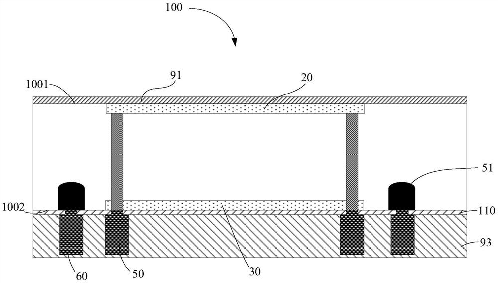
[0054] An embodiment of the present invention provides a photodiode, and the photodiode includes:

[0055]a substrate having opposing first and second surfaces, the material of which is a first conductivity type material;

[0056] A first doped region, loc...


PUM


Abstract

The invention provides a photodiode, a photodiode detector and a manufacturing method thereof. The photodiode comprises a substrate, a first doped region, a second doped region, a third doped region, an electrode wire, a dielectric layer and a first communicating hole, the substrate is provided with a first surface and a second surface which are opposite to each other, and the substrate is made of a first conductive type material; the first doped region is located in the substrate and is exposed from the first surface of the substrate; the first doped region is made of a second conductive type material; the second doped region is located in the substrate and is exposed from the second surface of the substrate; the second doped region is made of a second conductive type material; the dielectric layer is arranged on the second surface of the substrate; part of the electrode wire penetrates through the dielectric layer, the other part of the electrode wire is arranged on the side, away from the substrate, of the dielectric layer, and the electrode wire comprises a first electrode wire electrically connected with the second doped region; a first electric connecting column which is electrically connected with the first doped region and the first electrode wire is arranged in the first communicating hole; the third doped region is located in the substrate and exposed from the second surface of the substrate.

Description

technical field [0001] The invention belongs to the technical field of semiconductors, and in particular relates to a photodiode, a photodiode detector and a manufacturing method thereof. Background technique [0002] Compared with the traditional front-illuminated photodiode detector, the back-illuminated photodiode has the advantages of high mounting reliability, small pixel pitch, easy splicing, small crosstalk and good consistency in the application of array modules; due to the back-illuminated photodiode The space charge region of the substrate is located on the inner side close to the front side, and the substrate needs to be thinned to ensure that the light enters from the back side. In this way, it is easy to cause the absorption path of the incident light in the substrate to become smaller, especially the absorption efficiency of the long wave is reduced, so that the photogenerated carriers generated in the space charge region are reduced, resulting in the back-illu...

Claims


Application Information

Patent Timeline
IPC IPC(8): H01L27/146H01L31/0352
Inventor 樊堃祁春超仇筱乐刘艳丽
Owner HANGZHOU HIKVISION DIGITAL TECH
Why Eureka
Try Eureka