Magnetic field sensor, manufacturing process and magnetic field detection method thereof

A magnetic field sensor and detection method technology, applied in the field of magnetic sensors, can solve problems such as poor three-dimensional magnetic field detection effect, and achieve the effect of overcoming the poor effect and improving accuracy and precision

Pending Publication Date: 2022-04-19
GOERTEK MICROELECTRONICS CO LTD
0 Cites 0 Cited by

AI-Extracted Technical Summary

Problems solved by technology

[0003] The main purpose of this application is to provide a magnetic field sensor, manufacturing process and magnetic field detection method thereof, a...

Method used

In the present embodiment, specifically, on POI silicon wafer or SOI silicon wafer by PECVD (Plasma Enhanced Chemical Vapor Deposition, plasma enhanced chemical vapor deposition) equipment or ICPCVD (InductivelyCoupled Plasma Chemical Vapor Deposition, inductively coupled plasma chemical vapor deposition) equipment, etc. to deposit the first passivation layer to ensure that the magnetic unit and the base layer do not diffuse each other during the high-temperature rapid annealing process, and deposit the magnetic film by magnetron sputtering on the substrate with the passivation layer, and then Through high-temperature rapid annealing process such as RTP (rapid thermalprocessing, rapid thermal treatment), the magnetic moments in the magnetic film are ordered, the magnetic film layer is patterned to obtain a magnetic unit, and a second passivation layer is deposited on the magnetic unit , to separate the magnetic unit from the subsequently deposited magnetic induction thin film layer, avoiding the interface coupling effect affecting the performance of the magnetic unit, depositing the second passivation layer on the base by magnetron sputtering or evaporation and other methods to deposit a magnetic induction film, and then obtain a magnetic induction device with a Hall bar structure through a patterning process, and pattern the first passivation layer and the second passivation layer to reduce the stress of the film and avoid excessive stress from causing subsequent The produced MEMS (Micro-Electro-Mechanical System, micro-electro-mechanical system) structure undergoes warping deformation to obtain a standard magnetic field sensor capable of on-chip three-axis detection, wherein the passivation layer includes silicon nitride and/or silicon oxide etc., the patterning process includes steps such as spin coating, soft baking, exposure, post-baking, development, hard baking, etching and/or detection, wherein the magnetic film includes a permanent magnetic film, and the etching includes IBE (Ion BeamEtching, ion beam etching) or ICP (Inductively Coupled Plasma) etching, etc., the magnetic induction thin film layer is a multi-layer heterostructure based on the spin-orbit moment effect. In an implementable manner, the The multilayer heterostructure is Ta/CoFeB/MgO/Ta.
In this embodiment, specifically, on POI silicon wafer or SOI silicon wafer by PECVD (Plasma Enhanced Chemical Vapor Deposition, plasma enhanced chemical vapor deposition) equipment or ICPCVD (InductivelyCoupled Plasma Chemical Vapor Deposition, inductively c...

Abstract

The invention discloses a magnetic field sensor, a manufacturing process and a magnetic field detection method thereof, and the method comprises the following steps: manufacturing a sample magnetic field sensor, and enabling a magnetic induction device in the sample magnetic field sensor to be of a Hall rod structure; calibrating a standard change curve of the Hall resistance of the sample magnetic field sensor and the magnetic field intensity of each component; integrating a magnetic unit and the sample magnetic field sensor to obtain a standard magnetic field sensor; and detecting the actually-measured Hall resistance of the standard magnetic field sensor, inquiring the standard change curve according to the actually-measured Hall resistance, and determining the magnetic field intensity of each actually-measured component of the magnetic unit. The technical problem of poor high-precision three-dimensional magnetic field detection effect on the miniature magnetic unit in the prior art is solved, and the accuracy and precision of three-dimensional magnetic field detection on the miniature magnetic unit in the chip are greatly improved.

Application Domain

Single device manufacturingThree-component magnetometers

Technology Topic

Image

  • Magnetic field sensor, manufacturing process and magnetic field detection method thereof
  • Magnetic field sensor, manufacturing process and magnetic field detection method thereof

Examples

  • Experimental program(1)

Example Embodiment

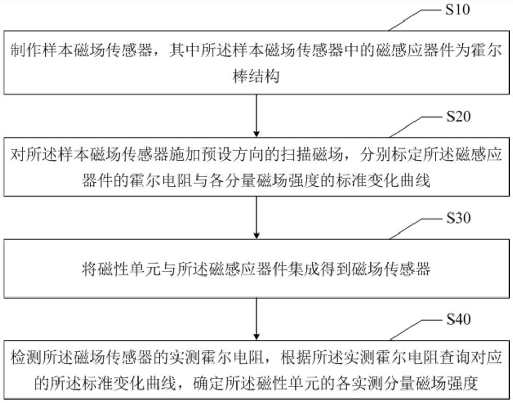
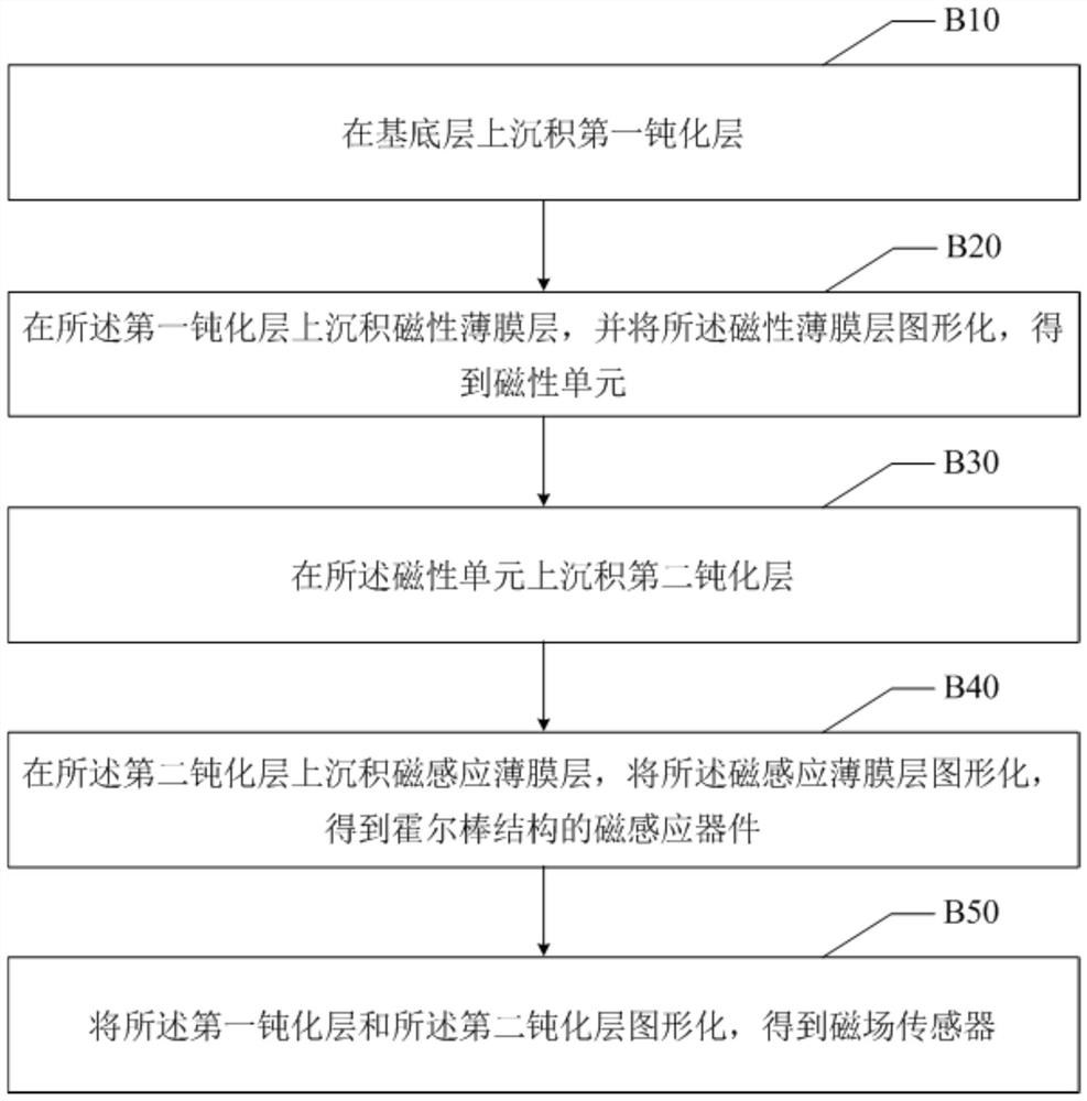
[0037] In order to make the above-described objects, features and advantages of the present invention can be more obvious and understandable, the following will be combined with the accompanying drawings in the embodiments of the present invention, the technical solutions in the embodiments of the present invention are clearly and completely described. Obviously, the embodiments described are only a portion of the embodiments of the present invention, and not all embodiments. Based on embodiments in the present invention, all other embodiments obtained by those of ordinary skill in the art without doing creative work, are within the scope of protection of the present invention.
[0038] High-precision magnetic field detection technology plays an important role in many application areas, such as navigation systems, automation equipment, biomedicine, etc., and the types of magnetic field sensors developed from this are becoming more and more abundant and more accurate, such as superconducting quantum interferometers, Hall sensors, magnetoresistive sensors (such as AMR (Anisotropic Magneto resistance, anisotropic magneto resistance) components, GMR (Giant Magneto resistance, Giant magnetoresistive) components and TMR (Tunnel MagnetoResistance, tunnel magnetoresistance) components, etc., greatly meet the needs of magnetic field detection in different working environments, even if the current magnetic field sensors are diverse, but are more limited to the detection of a large magnetic field space range, with the continuous development of spintronics, spintronics also came into being, such as MRAM (Magnetic Random Access Memory, Magnetic random access memory), spin chip, etc., and in the post-Moore era today, for some of the spintronic devices integrated in the chip with a small magnetic field space range (such as spin chips), the use of traditional external magnetic field sensors for detection means there are problems such as inaccurate detection points, low detection accuracy, etc. At present, although the integrated magnetic field detection in the chip has been realized, which greatly improves the detection accuracy, but for the use of magnetic flux aggregators, only GMR bar (giant magnetic resistance rod) is used. As a magnetic field induction unit to detect the magnetic field, can only detect the strength of the magnetic field in the xy plane, can not achieve the three-dimensional space in the x, y, z direction component magnetic field detection, and if the use of magnetic flux aggregator (such as: nickel-iron alloy materials), the x, y, z direction component magnetic field into the x and y direction, so as to achieve three-dimensional magnetic field uniaxial detection, the need for three different guides of the magnetic flux aggregator unit, because 1 magnetic flux aggregater and 1 GMR bar to form a single axis magnetic field detector, to detect x, y, The z-triaxial magnetic field requires three such uniaxial magnetic field detectors to be distributed near the target detection point, so there is not only the problem of inconsistent distribution points leading to large magnetic field errors, but also the problems of complex process production and large size of magnetic field induction units.
[0039] Embodiments of the present application provide a magnetic field detection method, in an embodiment of the magnetic field detection method of the present application, reference Figure 1 , the magnetic field detection methods include:
[0040] Step S10, make a sample magnetic field sensor, wherein the magnetic induction device in the sample magnetic field sensor is a Hall rod structure;
[0041] In the present embodiment, it should be noted that the magnetic field sensor is a device that can convert various magnetic fields and the amount of changes thereof into an electrical signal output, the standard magnetic field sensor comprises at least the base layer, a magnetic unit and a magnetic induction device, the sample magnetic field sensor comprises at least the base layer and a magnetic induction device, there is no magnetic element, the sample magnetic field sensor for determining the magnetic field to be measured in the absence of a magnetic field element to be measured, the magnetic induction device under the action of a scan magnetic field with a known magnetic field strength, the standard Hall resistance is generated, Further determine the magnetic induction device Hall resistance with each component magnetic field strength change curve, wherein the substrate may be SOI silicon wafer or POI silicon wafer, etc., the magnetic unit is deposited on the surface of the base layer, the magnetic unit comprises a permanent magnet, etc., the magnetic induction device is based on the spin orbital moment effect of a multilayer heterostructure, in an implementable manner, the multilayer heterostructure is Ta / CoFeB / MgO / Ta, the magnetic induction device is a Hall rod structure, The Hall rod structure consists of at least two Mutually Perpendicular Hall Rods, the magnetic induction device for detecting a three-dimensional magnetic field within the chip, the magnetic induction device is deposited on the substrate surface.
[0042] Specifically, the magnetic induction film layer is deposited on the substrate layer, the magnetic induction film layer is graphically obtained, to obtain a magnetic induction device of the Hall rod structure, wherein the base layer may be a SOI silicon wafer or POI silicon wafer, etc., the method of depositing the magnetic induction film layer comprises magnetron sputtering or evaporative deposition, etc., the method of patterning the magnetic induction film layer comprises lithography and etching and the like, specifically, the graphical process may also include rotational gluing, soft baking, exposure, post-baking, development, hard baking, etching and / or detection and other processes.
[0043] In one embodiment, the steps of making a sample magnetic field sensor comprising:
[0044] Deposition of a passivation layer on the basal layer;
[0045] Deposition of the magnetic induction thin film layer on the passivation layer, the magnetic induction film layer is graphically formulated, to obtain a magnetic induction device of hall rod structure;
[0046] The passivation layer is graphically presented to obtain a sample magnetic field sensor.
[0047] In the present embodiment, specifically, on the POI silicon wafer or SOI silicon wafer by PECVD (Plasma Enhanced Chemical Vapor Deposition) device or ICPCVD (InductivelyCoupled Plasma Chemical Vapor Deposition, inductively coupled plasma chemical vapor deposition) apparatus and the like deposition passivation layer, On the substrate deposited with a passivation layer by magnetic sputtering or evaporative deposition and other methods of deposition magnetic induction film, the magnetic induction film is graphically obtained to obtain a magnetic induction device of the Hall rod structure, wherein the passivation layer comprises silicon nitride and / or silicon oxide, etc., the graphical process comprises rotating gluing, soft baking, exposure, post-baking, development, hard baking, etching and / or detection and other processes, wherein the etching comprises IBE (Ion Beam Etching, ion beam etching) or ICP ( Inductively Couped Plasma) etching etc.
[0048] Step S20, the sample magnetic field sensor is applied to the scanning magnetic field in a preset direction, and the Hall resistance of the magnetic induction device and the standard change curve of the magnetic field strength of each component are calibrated, respectively;
[0049] In the present embodiment, it is emphasized that, if and only when the direction of the incoming current is collinear with the direction of the magnetic field in the surface, due to the spin orbital moment effect generates a spin orbital moment equivalent field perpendicular to the surface of the magnetic induction device, thereby driving the magnetic domain wall to move, the magnetic moment is flipped, and then directly contributed to the Hall resistance; when the current direction of the incoming current is orthogonal with the direction of the magnetic field in the plane, the magnetic domain wall will not be displaced, that is, it will not contribute to the Hall resistance; when the current is passed, there is no in-plane magnetic field, but there is an extra-plane magnetic field perpendicular to the plane, Magnetic domain wall will also occur displacement, thereby contributing to the Hall resistance, wherein the Hall resistance is the ratio of the Hall voltage to the incoming current, so the corresponding Hall resistance can be calculated by detecting the Hall voltage, and then in the sample magnetic field sensor without a magnetic unit, by applying a scanning magnetic field in a preset direction, detecting the Corresponding Hall resistance of the scanning magnetic field of different sizes of magnetic field strength, the Standard Change Curve of the Hall Resistance and the Magnetic Field Strength of Each Component can be obtained.
[0050] Wherein the scanning magnetic field is a series of magnetic field strength magnitude magnetic field, the standard change curve is the magnetic induction device under the action of a magnetic field of different magnetic field strength generated by the Hall resistance with the change of the magnetic field strength of the curve, the magnetic field strength of the component magnetic field is any direction of the magnetic field generated in a preset direction of the magnetic field strength, it is easy to understand that if the direction of the target magnetic field and the component magnetic field direction is the same, then the magnetic field strength of the component is equal to the magnetic field strength of the target magnetic field.
[0051] Specifically, the sample magnetic field sensor is applied to a scanning magnetic field in a preset direction, when a magnetic field of preset magnetic field strength is applied in each preset direction, a current is introduced into the preset current direction of the magnetic induction device, and then by detecting the voltage generated by the magnetic induction device, the corresponding Hall resistance is calculated according to the current and the voltage, and the Hall resistance and the corresponding preset magnetic field strength are recorded, The same preset direction of different magnetic field strength of the magnetic field action generated by the Hall resistance and each Hall resistance corresponding to the magnetic field strength of different sizes of statistical and curve fitting, you can obtain the magnetic induction device Hall resistance with the preset direction of the component magnetic field strength change standard change curve, wherein the preset direction comprises the magnetic induction device is located in the plane of the two directions perpendicular to each other, and perpendicular to the direction of the magnetic induction device where the plane, in order to facilitate the explanation, in the subsequent description process, In the x direction and y direction represents the magnetic induction device is located in the plane of the two directions perpendicular to each other, in the z direction represents the direction perpendicular to the plane where the magnetic induction device is located, e.g., along the x direction into the current Ix, the plane is applied in the x direction to apply a scanning magnetic field, the magnetic field of each magnetic field strength of the voltage Vy in the y direction generated by the magnetic induction device is recorded, and according to the Ix and Vy calculated to obtain the Hall resistance Rxy in the y direction, the Hx as the abscissa, Rxy as the vertical coordinate, The standard change curve of the Rxy with the change of Hx can be obtained.
[0052] Preferably, the magnetic field strength of the components comprises Hx in the x direction, hy in the y direction and Hz in the z direction, the Hall resistance comprising Rxy in the y direction and the Ryx in the x direction, the standard change curve comprising the Rxy-Hx curve and the Ryx-Hy curve, and the Rxy-Hz curve and / or Ryx-Hz curve, wherein the x direction and the y direction and the magnetic induction device coplanar, the x direction, the y direction and the z direction perpendicular to each other, The step of applying a scanning magnetic field in different directions to the sample magnetic field sensor, respectively calibrating the Hall resistance of the sample magnetic field sensor and the standard change curve of the magnetic field strength of each component comprises:
[0053] The sample magnetic field sensor is applied to a scanning magnetic field in a preset direction, respectively calibrated the Rxy-Hx curve and the Ryx-Hy curve of the magnetic induction device, and the Rxy-Hz curve and / or the Ryx-Hz curve.
[0054] In the present embodiment, specifically, the sample magnetic field sensor is applied to the scanning magnetic field in the x direction, the Rxy-Hx curve of the magnetic induction device is calibrated, the scanning magnetic field in the y direction is applied to the sample magnetic field sensor, the Ryx-Hy curve is calibrated to the magnetic induction device, the scanning magnetic field in the z direction is applied to the sample magnetic field sensor, the Rxy-Hz curve and / or the Ryx-Hz curve of the magnetic induction device is calibrated.
[0055] It is easy to understand that in order to carry out high-precision detection of the magnetic field strength of the component magnetic field in the x direction, y direction or z direction of the magnetic element, the magnetic field strength of the component in the corresponding direction and the standard change curve of the Hall resistance of the magnetic induction device, to achieve three-dimensional detection of the magnetic element, to obtain at least one of the magnetic induction device Hall resistance and x direction of the component magnetic field strength of the standard change curve, At least one of the Hall resistance of the magnetic induction device with the y direction of the component magnetic field strength of the standard change curve and at least one of the magnetic induction device Hall resistance and z direction of the component magnetic field strength of the standard change curve, e.g., to detect the magnetic field strength of the component of the magnetic element in the y direction, you need to calibrate the Ryx-Hy curve, to detect the magnetic field intensity within the plane of the magnetic element, you need to calibrate the Ryx-Hy curve and the Rxy-Hx curve, To detect the magnetic field strength of the magnetic unit in three dimensions, the Ryx-Hy curve and the Rxy-Hx curve need to be calibrated, and the Rxy-Hz curve and / or the Ryx-Hz curve.
[0056] Preferably, the preset direction comprises an x direction, the scanning magnetic field applied to the sample magnetic field sensor in a preset direction, the steps of calibrating the Rxy-Hx curve of the magnetic induction device comprising:
[0057] In the magnetic induction device along the x direction into a preset current, and the first scan magnetic field is applied in the x direction, the first scan magnetic field is detected to obtain the first Rxy corresponding to each Hx of the first scan magnetic field, to obtain an Rxy-Hx curve.
[0058] In the present embodiment, specifically, in the magnetic induction device along the x direction into a preset current, and along the x direction applied a first-scan magnetic field, the magnetic induction device in the first scanning magnetic field under the action of each of the first scanning magnetic field Hx magnetic field in the y direction of the voltage Vy, according to the preset current and detected the Vy can be calculated the magnetic induction device in the first scanning magnetic field of each Hx magnetic field generated by the first Rxy, Taking the first Rxy and the Hx as the horizontal ordinate coordinates, respectively, the Rxy of the magnetic induction device is obtained by the method of curve fitting with the component magnetic field strength of the x direction Hx-Hx curve of the Rxy-Hx curve.
[0059] Preferably, the preset direction comprises a y direction, the scanning magnetic field applied to the sample magnetic field sensor in a preset direction, the steps of calibrating the Ryx-Hy curve of the magnetic induction device comprising:
[0060] In the magnetic induction device along the y direction into a preset current, and a second sweep magnetic field is applied in the y direction, the first Ryx corresponding to each hy of the second scan magnetic field is detected, and the Ryx-Hy curve is obtained.
[0061] In the present embodiment, specifically, in the magnetic induction device along the y direction into a preset current, and a second scanning magnetic field is applied in the y direction, the magnetic induction device is detected in the first scanning magnetic field under the action of each hy magnetic field in the x direction of the voltage Vx, according to the preset current and detected the Vx can be calculated to obtain the magnetic induction device in the second scanning magnetic field under the magnetic field action of each hy of the first Ryx, Taking the first Ryx and the Hy as the horizontal ordinate coordinates, respectively, the Ryx of the magnetic induction device is obtained by the method of curve fitting with the component of the Ryx magnetic field in the y direction of the Ryx-Hy curve of the change of the magnetic field intensity Hy curve.
[0062] Preferably, the preset direction comprises a z-direction, the scanning magnetic field applied to the sample magnetic field sensor in a preset direction, the steps of calibrating the Rxy-Hz curve of the magnetic induction device comprising:
[0063] In the magnetic induction device along the x direction into a preset current, and a third sweep magnetic field is applied in the z direction, the second Rxy corresponding to each Hz of the third sweep magnetic field is detected, and the Rxy-Hz curve is obtained.
[0064] In the present embodiment, specifically, in the magnetic induction device along the x direction into a preset current, and along the z direction applied a third-scan magnetic field, the magnetic induction device in the first scanning magnetic field under the action of each Hz magnetic field in the y direction of the voltage Vy, according to the preset current and detected the Vy can be calculated to obtain the magnetic induction device in the third sweep magnetic field under the magnetic field action of each Hz of the second Rxy, Taking the second Rxy and the Hz as the horizontal ordinate coordinates, respectively, the Rxy of the magnetic induction device is obtained by the method of curve fitting with the component magnetic field intensity of the z direction Hz of the Rxy-Hz curve.
[0065] The preset direction comprises a z-direction, the sample magnetic field sensor is applied to a scan magnetic field of a preset direction, the steps of calibrating the Ryx-Hz curve of the magnetic induction device comprising:
[0066] In the magnetic induction device along the y direction into a preset current, and applied a fourth sweep magnetic field in the z direction, the second Ryx corresponding to each Hz of the fourth scan magnetic field is detected, to obtain a Ryx-Hz curve.
[0067] In the present embodiment, specifically, in the magnetic induction device along the y direction into a preset current, and a fourth scanning magnetic field is applied in the z direction, the magnetic induction device is detected in the first scanning magnetic field under the action of each Hz magnetic field in the x direction of the voltage Vx, according to the preset current and the detected Vx can be calculated to obtain the magnetic induction device in the fourth sweep magnetic field under the action of each Hz magnetic field generated by the second Ryx, Taking the second Ryx and the Hz as the horizontal ordinate coordinates, respectively, the Ryx of the magnetic induction device is obtained by the method of curve fitting with the component magnetic field strength of the z direction Hz Ryx-Hz curve.
[0068] Step S30, the magnetic unit is integrated with the sample magnetic field sensor to obtain a standard magnetic field sensor;
[0069] In the present embodiment, specifically, a magnetic film layer is deposited on the substrate layer, the magnetic film layer is graphically, a magnetic element is obtained, a magnetic induction film layer is deposited on the base layer at a preset distance of the magnetic unit, the magnetic induction film layer is patterned, a magnetic induction device of the Hall rod structure is obtained, wherein the base layer may be a SOI silicon wafer or a POI silicon wafer, etc., the magnetic film layer comprises a rare earth permanent magnet material or a ferrite permanent magnet material, etc., The method of depositing the magnetic thin film layer comprises magnetron sputtering or evaporative deposition, the method of patterning the magnetic thin film layer comprising lithography and etching processes, the magnetic induction thin film layer is a multilayer heterostructure based on the spin orbital moment effect, in an implementable manner, the multilayer heterostructure is Ta / CoFeB / MgO / Ta, the method of depositing the magnetic induction film layer comprises magnetron sputtering or evaporative deposition, etc., the method of patterning the magnetic induction film layer comprises lithography and etching processes, The magnetic induction device is a Hall rod structure, the Hall rod structure consists of at least two mutually perpendicular Hall rods, the distance between the magnetic unit and the magnetic induction device can be adjusted and disadvantages according to the magnetic field size and chip size at the time of actual application, etc., in this embodiment is not limited, in an embodiment, in a practicable manner, in the process of deposition and patterning of the magnetic film and the magnetic induction film, the base layer may also be deposited by depositing a passivation layer, The magnetic unit and the magnetic induction device are isolated and protected.
[0070] In one embodiment, the steps of integrating the magnetic unit with the sample magnetic field sensor to obtain a standard magnetic field sensor comprises:
[0071] Deposition of the first passivation layer on the basal layer;
[0072] Deposition of a magnetic thin film layer on the first passivation layer, and the magnetic thin film layer is graphically formulated to obtain a magnetic unit;
[0073] Deposition of a second passivation layer on the magnetic unit;
[0074] Deposition of the magnetic induction film layer on the second passivation layer, the magnetic induction film layer is graphically formulated, to obtain a magnetic induction device of Hall rod structure;
[0075] The first passivation layer and the second passivation layer are graphically formed to obtain a standard magnetic field sensor.
[0076] In the present embodiment, specifically, on the POI silicon wafer or SOI silicon wafer by PECVD (Plasma Enhanced Chemical Vapor Deposition) device or ICPCVD (InductivelyCoupled Plasma Chemical Vapor Deposition, inductively coupled plasma chemical vapor deposition) device deposition of the first passivation layer and the like to ensure that the magnetic unit and the base layer do not occur in the process of high temperature rapid annealing do not occur mutual diffusion, deposit the magnetic film by magnetron sputtering on the substrate deposited with the passivation layer, and then through the RTP (rapid thermalprocessing, rapid heat treatment) and other high temperature rapid annealing process, the magnetic moment in the magnetic film is ordered, the magnetic film layer is graphically obtained to obtain a magnetic element, the second passivation layer is deposited on the magnetic unit, To separate the magnetic element from the subsequent deposition of the magnetic induction film layer, to avoid the occurrence of interfacial coupling effect affecting the performance of the magnetic element, deposited magnetic induction film by magnetron sputtering or evaporative deposition on the base where the second passivation layer is deposited, and then by a graphical process to obtain a magnetic induction device of the Hall rod structure, the first passivation layer and the second passivation layer are graphically arranged, to reduce the stress of the film, to avoid stress over the ambassador subsequent production of MEMS ( Micro-Electro-Mechanical System, microelectromechanical system) structure warped deformation, to obtain a standard magnetic field sensor may be detected within the chip triaxial, wherein the passivation layer comprises silicon nitride and / or silicon oxide, etc., the graphical process comprises rotating gluing, soft baking, exposure, post-baking, developing, hard baking, etching and / or detection and other processes, wherein the magnetic film comprises a permanent magnet film, the etching comprises IBE (Ion). BeamEtching, ion beam etching) or ICP (Inductively Coupled Plasma) etching, the magnetic induction film layer is a multilayer heterostructure based on the spin orbital moment effect, in one embodiment, the multilayer heterostructure is Ta / CoFeB / MgO / Ta.
[0077] Step S40, the measured Hall resistance of the standard magnetic field sensor is detected, the measured Hall resistance is queried according to the corresponding standard change curve, and the magnetic field strength of each measured component of the magnetic unit is determined.
[0078] In the present embodiment, it should be noted that, in order to facilitate the explanation, in the x direction and y direction to represent the magnetic induction device in the plane of the two directions perpendicular to each other, in the z direction to represent the direction perpendicular to the plane where the magnetic induction device is located, assuming that the induction device in the three-dimensional vector magnetic field H (so that the x direction, y direction and z direction of the component magnetic field strength are Hx, Hy, Hz), the current is passed in the x + direction, then the Hall resistance Rxy measured in the y direction is determined by Hx and Hz together, If the current inflow direction is changed to along x-, the current in the opposite direction of the contribution to Rxy is opposite to the contribution to Rxy under the joint action of the same Hx, but the contribution to Rxy is unchanged under the joint action of Hz, so if the two are added, the Hx contribution is canceled, only the Hz contribution is contributed, and the contribution of Hz to Rxy is detected, that is, Rxy (Hz) = (Rxy1 + Rxy2)/2, if the two are subtracted, the Hz contribution is canceled, and only Hx contributes, thus detecting and isolating the contribution of Hx to Rxy, That is, Rxy(Hx) = (Rxy1-Rxy2)/2, in the same way, when the current is introduced in the y+ direction and the y- direction, the contribution of Hz to the Hall resistance Ryx measured in the x direction and the contribution of Hy to Ryx can be detected and separated, that is, Ryx (Hz) = (Ryx1 + Ryx2) / 2, Ryx (Hy) = (Ryx1-Ryx2) / 2.
[0079] Specifically, under the action of the magnetic field generated by the magnetic unit, a first current is passed into the positive direction of the preset current, by detecting the first voltage corresponding to the magnetic induction device, the corresponding first Hall resistance is calculated according to the first current and the first voltage, the second current is passed into the negative direction of the preset current, by detecting the second voltage corresponding to the magnetic induction device, the corresponding second Hall resistance is calculated according to the second current and the second voltage, According to the first Hall resistance and the second Hall resistance calculated to obtain a measured Hall resistance in the direction of the target resistance, according to the measured Hall resistance query corresponding to the standard change curve, you can obtain the magnetic element of the magnetic unit corresponding to the target magnetic field direction corresponding to the target magnetic field direction magnetic field strength, e.g., along the magnetic field sensing unit x + direction into the current + Ix, measured Vy1, calculated according to the +Ix and the Vy1 calculated to obtain Rxy1, and then in the x- direction into the current -Ix, Measured Vy2, calculated Rxy (Hxy) = (Rxy1-Rxy2) = (Rxy1-Rxy2)/2, according to the Rxy (Hx) query has been calibrated Rxy with Hx change standard change curve, read out the Hx value, that is, the permanent magnet x direction component magnetic field component, calculate Rxy (Hz) = (Rxy1 + Rxy2) / 2, according to the Rxy (Hz) query the calibrated Rxy-Hz curve, read out the Hz value, That is, the magnetic field component of the z-direction component of the permanent magnet.
[0080] Preferably, the measured Hall resistance of the detected standard magnetic field sensor, according to the measured Hall resistance query the standard change curve, the step of determining the magnetic field strength of each measured component of the magnetic unit comprises:
[0081] Step A10, the preset current is passed along the positive x direction, the measured preset current is generated Rxy1, the preset current is passed into the preset current in the negative direction of the x, the Rxy2 generated by the preset current is measured, the magnetic field of the x-direction component is determined according to the Rxy1 and the Rxy2 magnetic field generated by the magnetic induction device Rxy (Hx) and / or the z-direction component magnetic field generated by the magnetic induction device Rxy (Hz);
[0082] In the present embodiment, specifically, the preset current is passed in the positive direction of the x, the voltage of the preset current generated in the y direction is measured Vy1, the voltage generated by the preset current and the Vy1 is calculated according to the preset current and the Vy1 is calculated to obtain the Hall resistance Rxy1 generated by the magnetic field of the magnetic unit, the preset current is passed into the negative direction of the x, the voltage of the preset current generated in the y direction is measured Vy2, According to the preset current and the Vy2 calculated to obtain the magnetic induction device under the magnetic field action of the magnetic cell generated by the Hall resistance Rxy2, and then according to Rxy (Hx) = (Rxy1-Rxy2) / 2 calculation can be obtained Rxy (Hx), according to Rxy (Hz) = (Rxy1 + Rxy2) / 2 calculation can be obtained Rxy (Hz).
[0083] Step A20, the preset current is passed along the positive direction of the y, the Ryx3 generated by the measured preset current is measured, the preset current is passed into the negative direction of the y, the Ryx4 generated by the preset current is measured, the Ryx (Hz) generated by the magnetic field of the y-direction component is determined according to the Ryx3 and the Ryx4 of the magnetic field generated by the magnetic induction device and / or the z-direction component magnetic field is generated by the magnetic induction device;
[0084] In the present embodiment, specifically, the preset current is passed in the positive direction of the y, the voltage of the preset current generated in the x direction is measured Vx1, the magnetic induction device is calculated according to the preset current and the Vx1 is calculated to obtain the Hall resistance Ryx1 generated by the magnetic field of the magnetic unit, the preset current is passed into the negative direction of the y, the voltage of the preset current generated in the x direction is measured Vx2, According to the preset current and the Vx2 calculated to obtain the magnetic induction device under the magnetic field of the magnetic cell generated by the Hall resistance Ryx2, and then calculated according to Ryx (Hz) = (Ryx1 + Ryx2) / 2 can be calculated Ryx (Hz), according to Ryx (Hy) = (Ryx1-Ryx2) / 2 can be calculated to obtain Ryx (Hy).
[0085] Step A30, according to the Rxy (Hx) and Ryx (Hy), and Rxy (Hz) and / or Ryx (Hz) corresponding to the Rxy-Hx curve, the Ryx-Hy curve, the Rxy-Hz curve or the Ryx-Hz curve, respectively, according to the Rxy (Hx) and Ryx(Hy), respectively, according to the Rxy (Hx) and Ryx (Hy), and Rxy (Hz) and / or Ryx (Hz) corresponding to the Rxy-Hx curve, the Rxy-Hy curve, the Rxy-Hz curve or the Ryx-Hz curve, respectively, to obtain the magnetic field strength of the measured component in the x direction of the magnetic unit, the magnetic field strength of the measured component in the y direction and the magnetic field strength of the measured component in the z direction.
[0086] In the present embodiment, specifically, according to the Rxy (Hx) query corresponding to the Rxy-Hx curve, to obtain the magnetic field strength of the x-direction of the magnetic element, according to the Ryx (Hy) query corresponding to the Ryx-Hy curve, to obtain the magnetic field strength of the y-direction of the magnetic unit, according to the Rxy (Hz) query corresponding to the Rxy-Hz curve, to obtain the z-direction of the magnetic unit measured component magnetic field strength, according to the Ryx (Hz) Query the corresponding Ryx-Hz curve, to obtain the z-direction measured component magnetic field strength of the magnetic unit, it is easy to understand that the z-direction measured component magnetic field strength can be detected Rxy (Hz) and / or Ryx (Hz) and then query the corresponding standard change curve obtained, can be selected according to actual needs and presets, in this regard, the present embodiment is not limited.
[0087] In the present embodiment, by making a sample magnetic field sensor, wherein the magnetic induction device in the sample magnetic field sensor is a Hall rod structure, the sample magnetic field sensor is applied to the scanning magnetic field in a preset direction, respectively, the Hall resistance of the magnetic induction device and the standard change curve of the magnetic field strength of each component are calibrated, and the scanning magnetic field according to the autonomous application of different preset directions is realized, and the standard change curve of the magnetic field strength of the preset direction changes with the Hall resistance is established, By integrating the magnetic unit with the magnetic induction device to obtain a magnetic field sensor, by detecting the measured Hall resistance of the magnetic field sensor, querying the standard change curve according to the measured Hall resistance, determining the magnetic field strength of each measured component of the magnetic unit, and realizing the high-precision three-dimensional magnetic field detection of a single magnetic unit by a magnetic induction device integrated with the magnetic unit in the chip, That is, by using a magnetic induction device that integrates triaxial magnetic field detection based on the spin orbital moment effect as a magnetic field induction unit, the single magnetic unit in the chip is simply and accurately detected by electrical testing, which overcomes the technical problems of the poor effect of high-precision three-dimensional magnetic field detection of a single magnetic unit in the existing technology, and greatly improves the accuracy and accuracy of the three-dimensional magnetic field detection of the single magnetic unit in the chip.
[0088] Further, the present invention further provides a magnetic field sensor, the magnetic field sensor comprising: the base layer, a magnetic unit and a magnetic induction device; wherein the magnetic unit is deposited on the surface of the base layer, the magnetic induction device is a Hall rod structure, the magnetic induction device is deposited on the base layer surface.
[0089] In the present embodiment, it should be noted that the substrate may be SOI silicon wafer or POI silicon wafer, etc., the magnetic element is deposited on the surface of the base layer, the magnetic unit comprises a permanent magnet, etc., the magnetic induction device is a multilayer heterostructure based on the spin orbital moment effect, in one embodiment, the multilayer heterostructure is Ta / CoFeB / MgO / Ta, the magnetic induction device is a Hall rod structure, the Hall rod structure consists of at least two Mutually Perpendicular Hall Rods, The magnetic induction device for detecting the three-dimensional magnetic field within the chip, the magnetic induction device is deposited on the surface of the base layer.
[0090] Specifically, the magnetic field sensor manufacturing process comprises the following steps:
[0091] Deposition of the first passivation layer on the basal layer;
[0092] Deposition of a magnetic thin film layer on the first passivation layer, and the magnetic thin film layer is graphically formulated to obtain a magnetic unit;
[0093] Deposition of a second passivation layer on the magnetic unit;
[0094] Deposition of the magnetic induction film layer on the second passivation layer, the magnetic induction film layer is graphically formulated, to obtain a magnetic induction device of Hall rod structure;
[0095] The first passivation layer and the second passivation layer are patterned to obtain a magnetic field sensor.
[0096] Preferably, the magnetic induction film layer is Ta / CoFeB / MgO / Ta multilayer heterostructure.
[0097] In the present embodiment, by integrating a magnetic induction device having a spin orbital moment effect with the magnetic unit, the prior art of the micro magnetic unit for high-precision three-dimensional magnetic field detection effect is poor technical problems. Compared with the prior art, the present invention embodiments provide a beneficial effect of the magnetic field sensor and the above embodiments of the magnetic field detection method of the same beneficial effect, will not be repeated herein.
[0098] Further, reference Figure 2 , the present invention further provides a magnetic field sensor manufacturing process, the magnetic field sensor manufacturing process comprising the following steps:
[0099] Step B10, deposition of the first passivation layer on the basal layer;
[0100] Step B20, deposit the magnetic thin film layer on the first passivation layer, and the magnetic thin film layer is patterned to obtain a magnetic unit;
[0101] Step B30, deposit a second passivation layer on the magnetic unit;
[0102] Step B40, a magnetic induction thin film layer is deposited on the second passivation layer, the magnetic induction film layer is graphically formulated, and a magnetic induction device of hall rod structure is obtained;
[0103] Step B50, the first passivation layer and the second passivation layer are patterned to obtain a magnetic field sensor.
[0104] In the present embodiment, specifically, on the POI silicon wafer or SOI silicon wafer by PECVD (Plasma Enhanced Chemical Vapor Deposition) device or ICPCVD (InductivelyCoupled Plasma Chemical Vapor Deposition, inductively coupled plasma chemical vapor deposition) device deposition of the first passivation layer and the like to ensure that the magnetic unit and the base layer do not occur in the process of high temperature rapid annealing do not occur mutual diffusion, deposit the magnetic film by magnetron sputtering on the substrate deposited with the passivation layer, and then through the RTP (rapid thermalprocessing, rapid heat treatment) and other high temperature rapid annealing process, the magnetic moment in the magnetic film is ordered, the magnetic film layer is graphically obtained to obtain a magnetic element, the second passivation layer is deposited on the magnetic unit, To separate the magnetic element from the subsequent deposition of the magnetic induction film layer, to avoid the occurrence of interfacial coupling effect affecting the performance of the magnetic element, deposited magnetic induction film by magnetron sputtering or evaporative deposition on the base where the second passivation layer is deposited, and then by a graphical process to obtain a magnetic induction device of the Hall rod structure, the first passivation layer and the second passivation layer are graphically arranged, to reduce the stress of the film, to avoid stress over the ambassador subsequent production of MEMS ( Micro-Electro-Mechanical System, microelectromechanical system) structure warped deformation, to obtain a standard magnetic field sensor may be detected within the chip triaxial, wherein the passivation layer comprises silicon nitride and / or silicon oxide, etc., the graphical process comprises rotating gluing, soft baking, exposure, post-baking, developing, hard baking, etching and / or detection and other processes, wherein the magnetic film comprises a permanent magnet film, the etching comprises IBE (Ion). BeamEtching, ion beam etching) or ICP (Inductively Coupled Plasma) etching, the magnetic induction film layer is a multilayer heterogeneous structure based on the spin orbital moment effect, preferably, the magnetic induction film layer is Ta / CoFeB / MgO / Ta.
[0105] In the present embodiment, by integrating a magnetic induction device having a spin orbital moment effect with the magnetic unit, the technical problem of solving the technical problem of the prior art for high-precision three-dimensional magnetic field detection effect of the micro magnetic unit is solved. Compared with the prior art, the present invention embodiments provide a beneficial effect of the magnetic field sensor and the above embodiments of the magnetic field detection method of the same beneficial effect, will not be repeated herein.
[0106] The above is only a preferred embodiment of the present application, and does not therefore limit the patent scope of the present application, where the equivalent structure or equivalent process transformation made by using the contents of the present application specification and drawings, or directly or indirectly applied in other relevant technical fields, is the same reason included in the patent processing scope of this application.

PUM

no PUM

Description & Claims & Application Information

We can also present the details of the Description, Claims and Application information to help users get a comprehensive understanding of the technical details of the patent, such as background art, summary of invention, brief description of drawings, description of embodiments, and other original content. On the other hand, users can also determine the specific scope of protection of the technology through the list of claims; as well as understand the changes in the life cycle of the technology with the presentation of the patent timeline. Login to view more.

Similar technology patents

Pretreatment kit for salbutamol sample based on immunomagnetic beads

PendingCN108508199AReduce interference from background substancesImprove accuracy and precisionMaterial analysisChemistryImmunomagnetic bead
Owner:沭阳康源泰博生物科技有限公司

Classification and recommendation of technical efficacy words

Why Eureka
Try Eureka