Supercharge Your Innovation With Domain-Expert AI Agents!

A method and system for obtaining an optical proximity effect correction model

A technology for optical proximity effect and model correction, which is applied in optics, originals for opto-mechanical processing, and photoengraving of patterned surfaces. Avoid the effects of the winger effect

Active Publication Date: 2022-07-05
NEXCHIP SEMICON CO LTD
View PDF4 Cites 0 Cited by
  • Summary
  • Abstract
  • Description
  • Claims
  • Application Information

AI Technical Summary

Problems solved by technology

As a result, the pattern formed on the final wafer is different from the design pattern
Moreover, the probability of the winger effect is random, and it will consume a lot of manpower and time during detection

Method used


Image

  • A method and system for obtaining an optical proximity effect correction model
  • A method and system for obtaining an optical proximity effect correction model
  • A method and system for obtaining an optical proximity effect correction model

Examples


Embodiment Construction

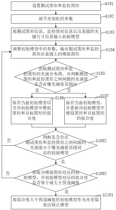
[0049] The technical solutions in the embodiments of the present invention will be clearly and completely described below with reference to the accompanying drawings in the embodiments of the present invention. Obviously, the described embodiments are only a part of the embodiments of the present invention, but not all of the embodiments. Based on the embodiments of the present invention, all other embodiments obtained by those of ordinary skill in the art without creative efforts shall fall within the protection scope of the present invention.

[0050] In the manufacturing process of the semiconductor integrated circuit, the circuit design is firstly carried out, and then the circuit design scheme is subjected to layout design to form a layout pattern, for example, the layout pattern is transferred to the mask through a phase shift mask. Specifically, for example, the layout pattern can be exposed by an electron beam exposure machine, and the pattern can be exposed to a mask o...


PUM


Abstract

The invention discloses a method and system for obtaining an optical proximity effect correction model, which comprises the following steps: establishing an initial model; setting a test pattern, and setting a monitoring pattern on one side of the test pattern, and the test pattern and all There is a gap between the monitoring patterns; the exposure threshold range of the lithography machine is obtained; the parameters in the initial model are adjusted, the test pattern and the monitoring pattern are corrected, and the light of the test pattern and the monitoring pattern is obtained. Intensity distribution diagram, and the simulation pattern of the test pattern and the monitoring pattern on the wafer; and the light intensity value of the gap is less than the exposure threshold range, and the simulation pattern and the target pattern when the fitting degree is the highest The initial model, as the optical proximity effect correction model. The method and system for obtaining an optical proximity effect correction model provided by the present invention can improve the accuracy of the semiconductor manufacturing process.

Description

technical field [0001] The invention belongs to the field of integrated circuit manufacturing, and in particular relates to a method and system for obtaining an optical proximity effect correction model. Background technique [0002] With the development of the semiconductor manufacturing industry, when the layout is transferred to the mask and then to the wafer, the requirements for resolution are getting higher and higher. The type of resist and mask improves resolution. [0003] Phase Shift Mask (PSM) is a resolution enhancement technology that uses the intensity and phase of light to image at the same time to obtain higher resolution. When using the phase-shift mask technology for pattern transfer, the use of the phase-shift mask tends to form a small peak of light intensity on the dark side of the edge of the design pattern, called a side-lobe. Under stronger exposure energy, the energy of the edge may be greater than the threshold of photoresist exposure. When the ed...

Claims


Application Information

Patent Timeline
Patent Type & Authority Patents(China)
IPC IPC(8): G03F1/36
CPCG03F1/36
Inventor 王康罗招龙吴晨雨杜宇
Owner NEXCHIP SEMICON CO LTD
Features
  • R&D
  • Intellectual Property
  • Life Sciences
  • Materials
  • Tech Scout
  • Unparalleled Data Quality
  • Higher Quality Content
  • 60% Fewer Hallucinations
Learn More