Preparation method of semiconductor device and semiconductor device
A semiconductor and device technology, which is applied in the preparation of semiconductor devices and the field of semiconductor devices, can solve the problems that Wafer central GaN and edge GaN cannot be etched at the same time, the etching speed of the edge and the center is inconsistent, and the performance of the device is affected. Achieve the effect of avoiding back hole metal layering, avoiding back hole collapse, and ensuring device yield
- Summary
- Abstract
- Description
- Claims
- Application Information
AI Technical Summary
Problems solved by technology
Method used
Image
Examples
no. 1 example
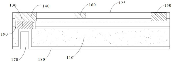
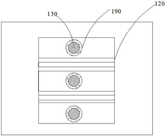
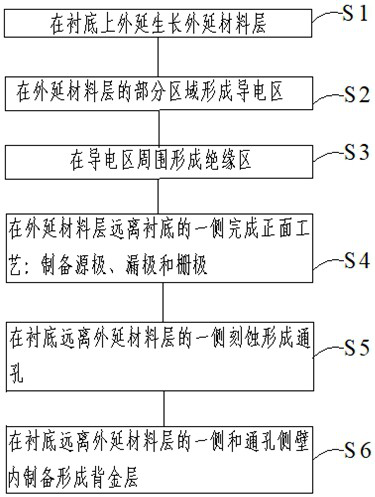
[0061] see figure 1 , this embodiment provides a method for preparing a semiconductor device 100 for preparing the semiconductor device 100 , the method does not have the problem of over-etching after the etching is completed, and avoids the possible collapse of the back hole and the occurrence of the over-etching process. Technical problems such as back hole metal delamination ensure the device yield and device performance.
[0062] The manufacturing method of the semiconductor device 100 provided in this embodiment includes the following steps:
[0063] S1 : epitaxially growing the epitaxial material layer 120 on the substrate 110 .
[0064] see in combination figure 2 Specifically, the nucleation layer 121, the first epitaxial layer 122, the second epitaxial layer 123 and the cap layer 124 may be sequentially deposited on the substrate 110 by MOCVD (chemical vapor deposition), wherein the substrate 110 may be SiC, Si, Sapphire, etc., preferably SiC, the nucleation layer...
no. 2 example
[0084] see Figure 10 , this embodiment provides a method for fabricating a semiconductor device 100, the basic steps, processes and technical effects of the method are the same as those in the first embodiment. Corresponding content in the examples.
[0085] This embodiment provides a method for fabricating a semiconductor device 100, including the following steps:
[0086] S1 : epitaxially growing the epitaxial material layer 120 on the substrate 110 .
[0087] Specifically, the nucleation layer 121 , the first epitaxial layer 122 , the second epitaxial layer 123 and the cap layer 124 may be sequentially deposited on the substrate 110 by MOCVD (Chemical Vapor Deposition). After the epitaxial material layer 120 is formed, a passivation layer 125 can also be grown on the surface of the epitaxial material layer 120. The passivation layer 125 can be made of SiN, and SiN forms dangling bonds with the surface of the material to achieve surface passivation and solve the current p...
no. 3 example
[0103] see Figure 14 , this embodiment provides a method for fabricating a semiconductor device 100, the basic steps, processes and technical effects are the same as those in the second embodiment. For a brief description, for the parts not mentioned in this embodiment, refer to the second Corresponding content in the examples.
[0104] This embodiment provides a method for fabricating a semiconductor device 100, including the following steps:
[0105] S1 : epitaxially growing the epitaxial material layer 120 on the substrate 110 .
[0106] S2 : forming a conductive region 130 in a partial region of the epitaxial material layer 120 .
[0107] Specifically, the first implantation region may be formed in a partial region of the epitaxial material layer 120 by Si ion implantation, and then the first implantation region may be activated after high temperature annealing to form the conductive region 130 .
[0108] Wherein, steps S1-step S2 are the same as those in the second em...
PUM
 Abstract
Description
Claims
Application Information
 - R&D
- Intellectual Property
- Life Sciences
- Materials
- Tech Scout
- Unparalleled Data Quality
- Higher Quality Content
- 60% Fewer Hallucinations
Browse by: Latest US Patents, China's latest patents, Technical Efficacy Thesaurus, Application Domain, Technology Topic, Popular Technical Reports.
© 2025 PatSnap. All rights reserved.Legal|Privacy policy|Modern Slavery Act Transparency Statement|Sitemap|About US| Contact US: help@patsnap.com


