Silicon pressure transducer chip and method based on silicon-silicon linking and silicon-on-insulating layer

A sensor chip, silicon-silicon bond technology, applied to the process for producing decorative surface effects, piezoelectric/electrostrictive/magnetostrictive devices, measurement of the properties and forces of piezoelectric resistance materials, etc., can solve the problem It is difficult to ensure the uniformity of the film and other problems, so as to achieve the effect of ensuring long-term stability, good process repeatability and stability, and product yield guarantee

Inactive Publication Date: 2008-09-24
SHANGHAI INST OF MICROSYSTEM & INFORMATION TECH CHINESE ACAD OF SCI
View PDF0 Cites 25 Cited by
  • Summary
  • Abstract
  • Description
  • Claims
  • Application Information

AI Technical Summary

Problems solved by technology

However, due to the need for long-term anisotropic etching to achieve ultra-thin stress films during the preparation process, it is difficult to ensure the uniformity of different positions of the film and between different batches of films, so for large-scale production There are also limitations

Method used


Image

  • Silicon pressure transducer chip and method based on silicon-silicon linking and silicon-on-insulating layer
  • Silicon pressure transducer chip and method based on silicon-silicon linking and silicon-on-insulating layer
  • Silicon pressure transducer chip and method based on silicon-silicon linking and silicon-on-insulating layer

Examples


Embodiment Construction

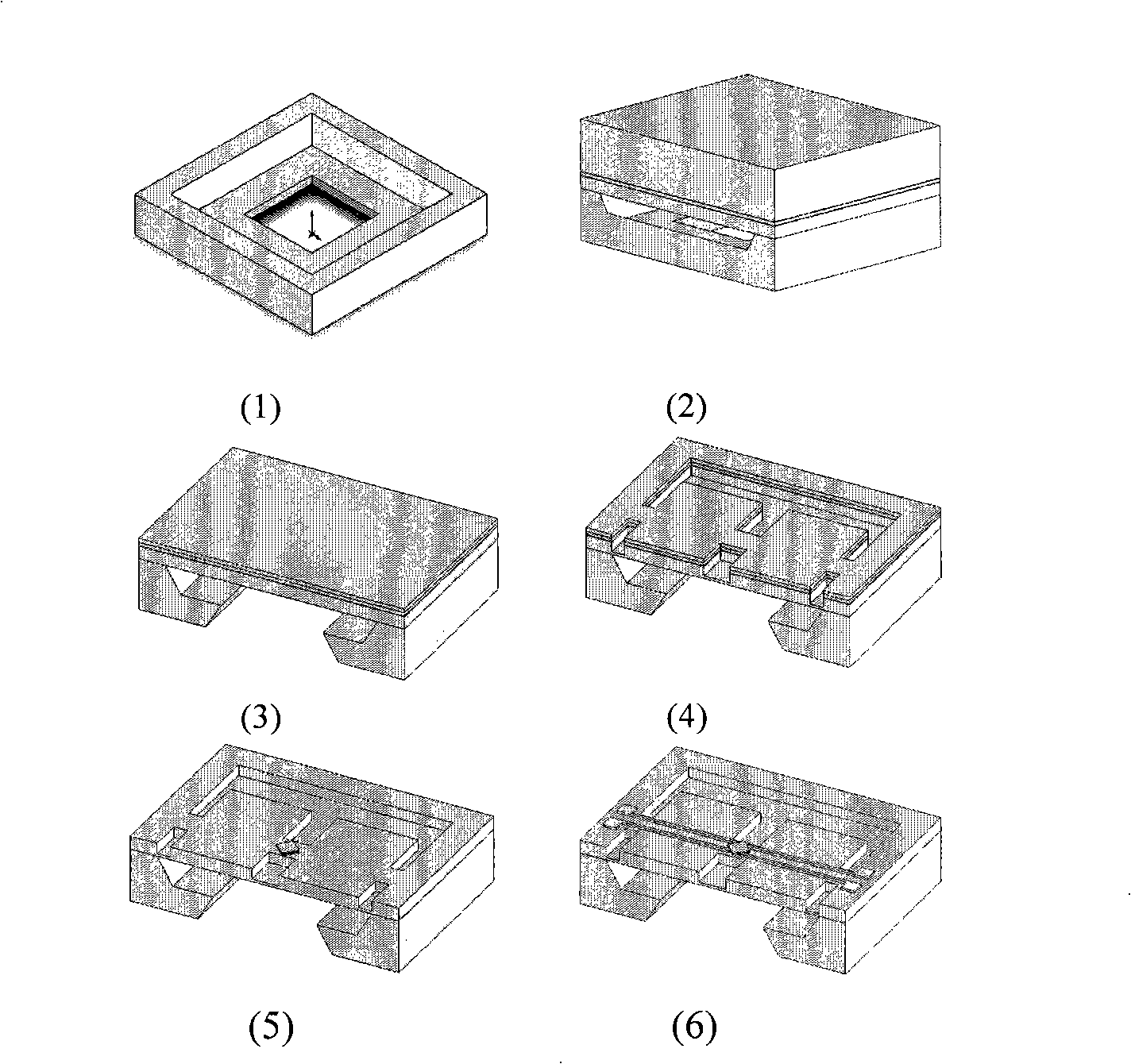
[0019] The following examples will help to understand the present invention, but do not limit the content of the present invention. The manufacturing method of the pressure sensor chip based on silicon-silicon bonding and silicon-on-insulator suitable for the 1KPa range:

[0020] Use 4-inch 450μm N-type (100) double-polished single-crystal silicon wafers with a resistivity of 1-10ohm.cm, and 4-inch P-type double-polished SOI wafers. The thickness of the top silicon layer and the buried layer are 30μm and 1μm respectively. Silicon resistivity 1-10ohm.cm.

[0021] 1. The silicon wafer is cleaned and then oxidized, and shallow grooves and air guide holes are etched in the potassium hydroxide solution. The depth of the shallow grooves is 15 μm, such as figure 2 as shown in (1);

[0022] 2. SOI wafers and silicon wafers are bonded on the shallow groove surface. Use 400°C vacuum in the bonding machine, pressurize 2bar for 20 minutes, and then dry oxygen in a 1200°C high-temperatu...


PUM

PropertyMeasurementUnit
thicknessaaaaaaaaaa
thicknessaaaaaaaaaa
Sensitivityaaaaaaaaaa

Abstract

The invention relates to a pressure sensor chip based on silicon direction bonding and silicon on insulator and a manufacturing method thereof, and belongs to the field of sensor chips. The invention is characterized in that a shallow slot and a gas port on a supporting silicon wafer are formed through anisotropy corrosion, and appropriate shallow slot depth obtained by controlling the corrosion time can realize over pressure protection of parts. A silicon direct bonding technology bonds the supporting wafer and a reversed SOI wafer, realizes a beam-membrane structure on the SOI after lapping and polishing to improve the sensitivity and linearity of the parts; manufactures force sensing resistance elements on the processed beam; adopts the oxidation buried layer of the SOI to solve insulation and isolation of the sensing elements and elastic elements; and improves the long-termed reliability and adaptability under high temperature of the parts. The SOP high-sensitivity pressure sensor chip based on the bonding technology has the advantages of controllable process, excellent repeatability and high finished product rate.

Description

technical field [0001] The invention relates to a high-sensitivity and low-range pressure sensor chip based on silicon-silicon bonding technology and silicon-on-insulator (SOI) and a manufacturing method thereof, belonging to the field of sensor chips. Background technique [0002] Silicon-based pressure sensors, as the most commercially successful micro-electromechanical systems (MEMS) devices, have been widely used and improved in the fields of petroleum, aerospace, medical equipment, and automotive electronics in the past few decades. However, since the bulk silicon pressure sensor prepared by silicon micromachining technology uses pn junction as the electrical isolation method, it will fail due to the increase of reverse leakage current in the environment above 125°C; ordinary pressure sensors usually use the aspect ratio of the stress film It is made large enough to obtain high sensitivity, but in low-range applications, this design will deteriorate the linear character...

Claims


Application Information

Patent Timeline
Patent Type & Authority Applications(China)
IPC IPC(8): G01L1/18B81B7/02B81C1/00
Inventor 武爱民陈静王曦魏星张波
Owner SHANGHAI INST OF MICROSYSTEM & INFORMATION TECH CHINESE ACAD OF SCI
Why Eureka
Try Eureka