Active organic light-emitting diode (OLED) display device and manufacturing method thereof

A display device and active technology, which is applied in semiconductor/solid-state device manufacturing, electric solid-state devices, semiconductor devices, etc., can solve the problems of light extraction rate and process, low contact resistance of cathode and cathode power line, etc. The effect of extraction rate, reduction of contact resistance, and simple preparation process

Active Publication Date: 2013-08-21
KUNSHAN NEW FLAT PANEL DISPLAY TECH CENT
View PDF5 Cites 24 Cited by
  • Summary
  • Abstract
  • Description
  • Claims
  • Application Information

AI Technical Summary

Problems solved by technology

[0010] For this reason, what the present invention is to solve is the problem that the method for reducing the contact resistance of the cathode and the cathode power supply line in the top-emitting OLED affects the light output rate and the problem that the process is complicated and difficult to realize, and provides an active OLED display with a low contact resistance between the cathode and the cathode power supply line Devices and methods of making them

Method used


Image

  • Active organic light-emitting diode (OLED) display device and manufacturing method thereof
  • Active organic light-emitting diode (OLED) display device and manufacturing method thereof
  • Active organic light-emitting diode (OLED) display device and manufacturing method thereof

Examples


Embodiment 1

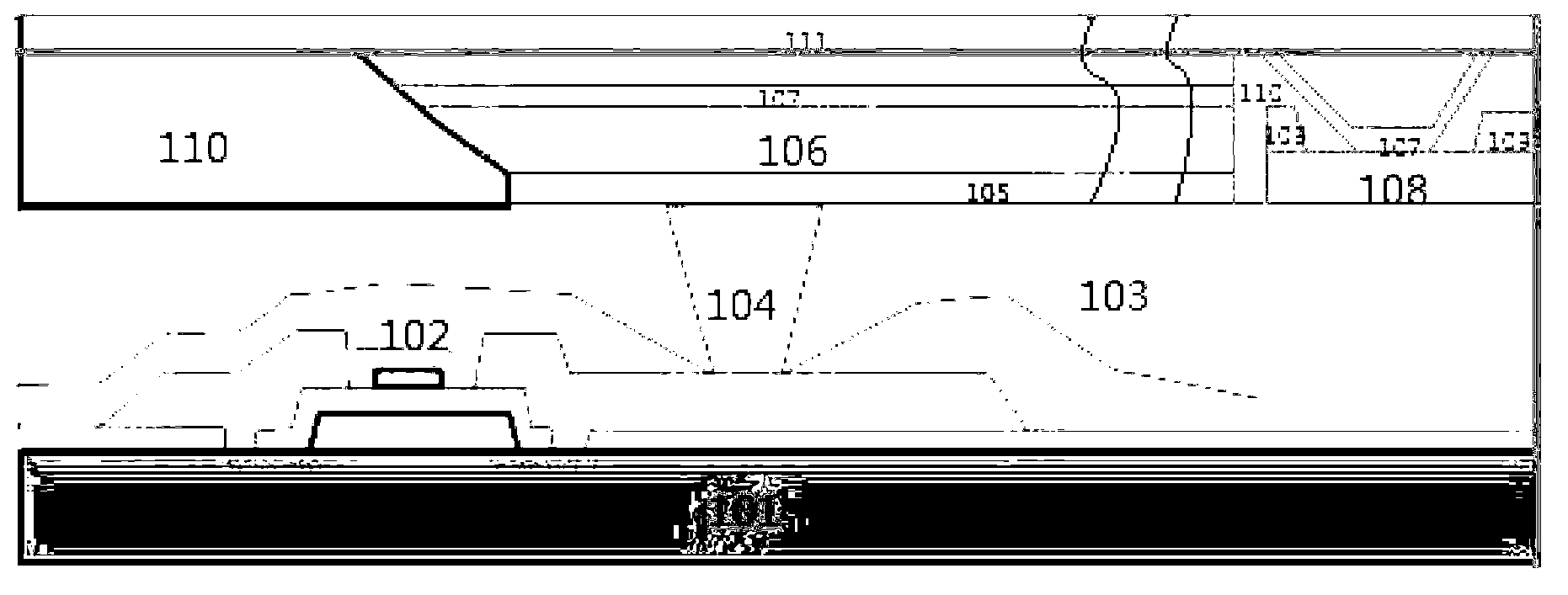
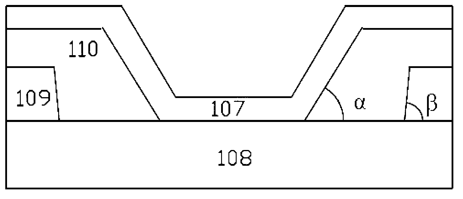
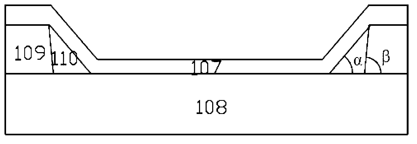
[0044] This embodiment provides an active OLED display device, as attached figure 1 and Figure 2a As shown, it includes a display area and a non-display area. The display area includes an anode, an organic functional layer and a cathode. The non-display area includes a cathode power line 108. An insulating layer 109 is arranged on the cathode power line 108. The cathode 107 covers the insulating layer 109. The insulating layer 109 is provided with a contact hole for connecting the cathode 107 and the cathode power supply line 108, and the insulating layer 109 is also covered with a planarization layer 110, and the planarization layer 110 extends to cover the cathode power supply line 108, and leaves a cathode The contact hole between 107 and the cathode power supply line 108, the slope angle α formed by the contact surface of the planarization layer 110 and the cathode power supply line 108 is 60°. A planarization layer 110 is covered on the insulating layer 109 partially d...

Embodiment 2

[0061] This embodiment provides an active OLED display device, as attached figure 1 and 2b As shown, the structure and manufacturing method of the active OLED display device are the same as those in Embodiment 1, the only difference is that the slope angle formed by the planarization layer 110 covering the insulating layer is α is 45 degrees.

Embodiment 3

[0063] This embodiment provides an active OLED display device. The structure and manufacturing method of the active OLED display device are the same as those in Embodiment 1, the only difference being that the slope angle α formed by the planarization layer and the contact surface of the cathode power line is 30°.


PUM


Abstract

The invention provides an active organic light-emitting diode (OLED) display device and a manufacturing method thereof. The active OLED display device comprises a display area and a non-display area. The non-display area comprises a negative electrode power line, wherein an insulating layer is arranged on the negative electrode power line, a planarization layer further covers the insulating layer and extends to and covers the negative electrode power line, and a gradient included angle alpha formed by the planarization layer and the contact surface of the negative electrode power line is smaller than a gradient included angle beta formed by the insulating layer and the contact surface of the negative electrode power line, so transition is flatly and slowly formed from a negative electrode to the negative electrode power line, smoothness from the negative electrode to the contact area of the negative electrode power line is increased, and contact resistance is effectively reduced. The planarization layer covers a non-pixel area of a positive electrode, and the thickness of the planarization layer is larger than or equal to the sum of the thickness of the positive electrode, the thickness of an organic functional layer and the thickness of the negative electrode, so a pixel area can be protected against scratching, the rate of finished products of the display device is effectively guaranteed, a manufacturing process is simple, and the process is easy to achieve.

Description

technical field [0001] The invention relates to the field of organic electroluminescence, in particular to an active OLED display device. Background technique [0002] Organic light-emitting display diode (English full name Organic Light-Emitting Diode, referred to as OLED) is an active light-emitting device. Compared with thin-film transistor liquid crystal display (English full name Liquid Crystal Display, LCD for short) and plasma display panel (English full name Plasma Display Panel, PDP) in the existing flat panel display technology, OLED has high contrast, wide viewing angle, low power consumption, and small size. It is expected to become the mainstream flat panel display technology of the next generation, and it is one of the most concerned technologies in the flat panel display technology at present. [0003] According to the driving method, organic light-emitting display devices can be divided into passively driven organic light-emitting devices (English full name:...

Claims


Application Information

Patent Timeline
Patent Type & Authority Applications(China)
IPC IPC(8): H01L51/52H01L27/32H01L51/56
Inventor 陈红邱勇黄秀颀敖伟
Owner KUNSHAN NEW FLAT PANEL DISPLAY TECH CENT
Why Eureka
Try Eureka