
Automatic chip discharging and conveying device

A technology of automatic unloading and conveying device, applied in the direction of conveyor objects, transportation and packaging, electrical components, etc., to achieve the effect of stable connection

Pending Publication Date: 2022-05-10
苏州声芯电子科技有限公司
View PDF0 Cites 3 Cited by
  • Summary
  • Abstract
  • Description
  • Claims
  • Application Information

AI Technical Summary

Problems solved by technology

[0002] In a broad sense, the chip is actually a packaged chip formed after packaging. The chip body is placed on the carrier table and then bonded. Bonding is to combine two homogeneous or heterogeneous semiconductor materials with clean surfaces and atomic level flatness Surface cleaning and activation treatment, direct bonding under certain conditions, the technology of bonding chips into one through van der Waals force, molecular force or even atomic force; chip bonding needs to be produced in batches, so the chip is put into the bonding process in preparation for bonding. In the corresponding carrier, place the carrier on the carrier table that can be bonded. After the bonding is completed, manually remove the carrier to the carrier storage box, and finally fill the carrier storage box by the worker. Remove it from the station and replace it with an empty carrier storage box. The carrier storage box includes a box body, one side of the box body is open and a baffle is slidably installed, the upper end of the box body is provided with a box body handle, and the box body is provided with There are a number of slots for placing carriers. At present, there is no automatic device that can replace the manual loading of the carrier and put the carrier into the carrier receiving box after the bonding is completed, and it can also carry out the loading. Delivery with container

Method used


Image

  • Automatic chip discharging and conveying device
  • Automatic chip discharging and conveying device
  • Automatic chip discharging and conveying device

Examples


Embodiment Construction

[0035] The present invention will be described in further detail below through specific examples.

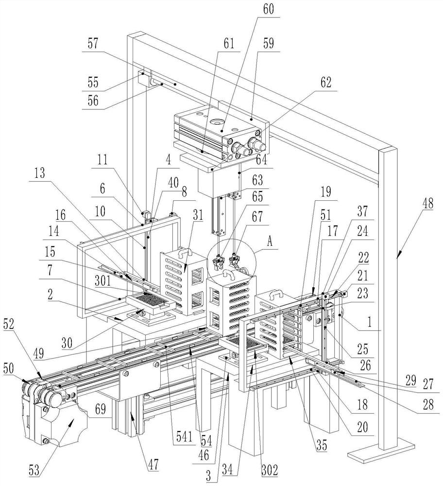
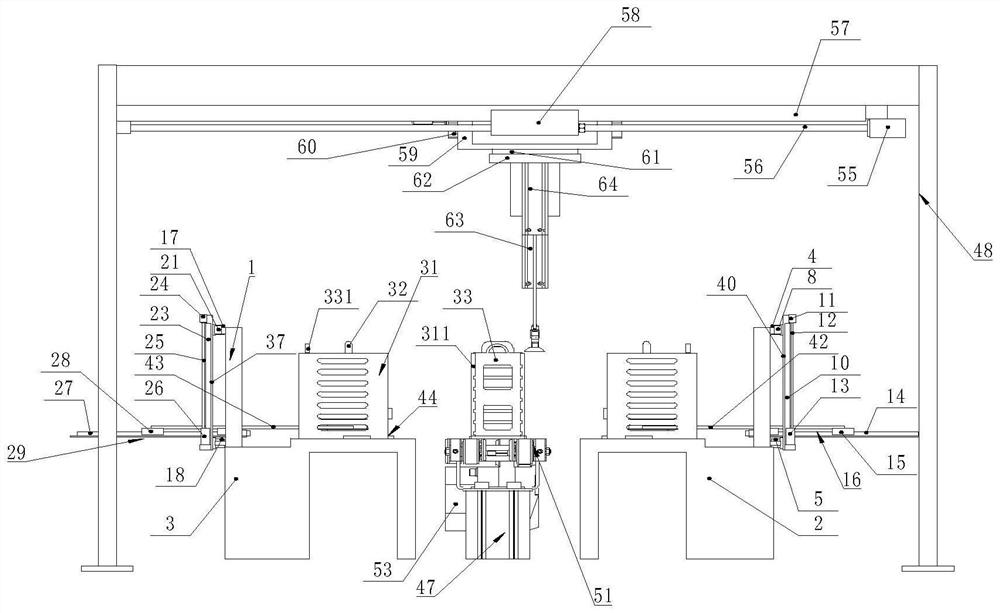
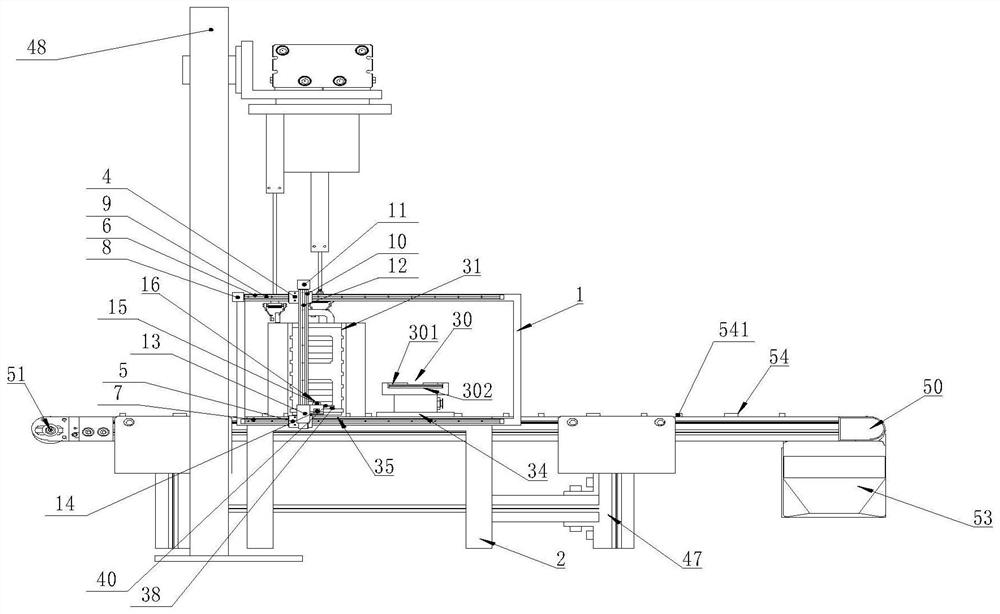
[0036] Such as Figure 1 to Figure 7 As shown, an automatic chip unloading and conveying device includes a chip carrier transfer device and a storage box transfer device, and the chip carrier transfer device includes an adsorption support frame 1, a carrier table 30, and a carrier storage box 31 and the workbench, the carrier table 30 and the carrier accommodating box 31 are respectively placed on the bonding station 34 and the adsorption station 35 on the workbench, the carrier table 30 is provided with an opening groove 301, and the opening The feeding end of the groove 301 is provided with an assembly port 302 for easy extraction of the carrier; the carrier receiving box 31 is provided with several carrier receiving grooves 311 for inserting the carrier, and the adsorption support frame 1 is fixedly installed with An X guide rail extending along the horizontal X direction, o...


PUM


Abstract

The invention discloses an automatic chip discharging and conveying device which comprises a chip carrier transferring and conveying device and a containing box transferring and conveying device, the chip carrier transferring and conveying device comprises an adsorption supporting frame, a carrier table, a carrier containing box and a workbench, and the carrier table and the carrier containing box are placed on a bonding station and an adsorption station on the workbench respectively. An opening groove is formed in the carrier table, and an assembling opening facilitating pulling out of the carrier is formed in the feeding end of the opening groove. The carrier containing box is provided with a plurality of carrier containing grooves used for insertion of carriers, the device can automatically clamp the carrier containing box filled with the carriers which are not bonded to an adsorption station, the carriers are taken out of the carrier containing box one by one through a machine, and after bonding is completed, the carriers are put back into the carrier containing box. And then the carrier containing box filled with the bonded carriers is clamped to the conveying belt to be conveyed to the next working procedure, so that the labor force is reduced, and the production efficiency is improved.

Description

technical field [0001] The invention relates to an automatic chip feeding and conveying device, which is suitable for production in the field of semiconductor chip manufacturing. Background technique [0002] In a broad sense, a chip is actually a packaged chip formed after packaging. The chip body is placed on the carrier stage and then bonded. Bonding is to combine two homogeneous or heterogeneous semiconductor materials with clean surfaces and atomic level flatness Surface cleaning and activation treatment, direct bonding under certain conditions, the technology of bonding chips into one through van der Waals force, molecular force or even atomic force; chip bonding needs to be produced in batches, so the chip is placed in the process of preparing for bonding. In the corresponding carrier, place the carrier on the carrier table that can be bonded. After the bonding is completed, manually remove the carrier to the carrier storage box, and finally fill the carrier storage b...

Claims


Application Information

Patent Timeline
Patent Type & Authority Applications(China)
IPC IPC(8): H01L21/677
CPCH01L21/6773H01L21/67736H01L21/67706
Inventor 张啸云蒋云武
Owner 苏州声芯电子科技有限公司
Learn More