Reverse conducting IGBT

A reverse-conducting, conductive-type technology, applied in semiconductor devices, diodes, electrical components, etc., can solve the problems of increasing IGBT saturation voltage, difficulty in balancing, and conflict, and achieve charge balance, saturation voltage drop optimization, and good emission. The effect of efficiency

Pending Publication Date: 2022-05-10
上海擎茂微电子科技有限公司
View PDF0 Cites 2 Cited by
  • Summary
  • Abstract
  • Description
  • Claims
  • Application Information

AI Technical Summary

Problems solved by technology

At the same time, the global lifetime control in order to reduce the FRD reverse recovery charge will inevitably increase the saturation voltage of the IGBT
Moreover, FRD needs a certain area to reduce Vf, which also means that IGBT needs to lose these areas
[0003] Generally speaking, its problem is mainly that the parameters in the optimization performance of IGBT and FRD conflict with each other, and it is difficult to balance

Method used


Image

  • Reverse conducting IGBT
  • Reverse conducting IGBT

Examples


Embodiment Construction

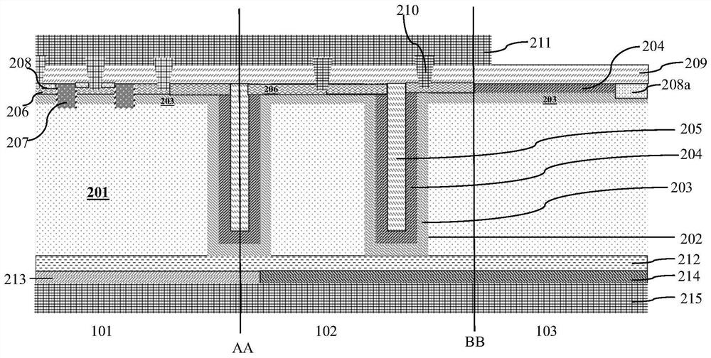
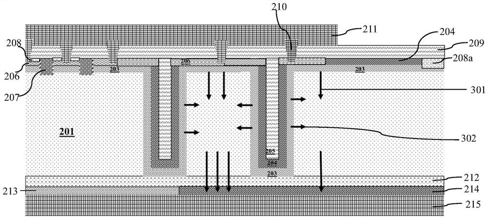
[0051] like figure 1 Shown is a schematic structural diagram of the reverse conduction IGBT of the embodiment of the present invention; the reverse conduction IGBT of the embodiment of the present invention includes an antiparallel IGBT and an FRD.

[0052] In the lateral direction, the formation region 101 of the IGBT and the formation region 102 of the FRD are adjacent to and separated from each other. figure 1 In the figure, the IGBT formation area 101 is located on the left side of the line AA; the FRD formation area 102 is located between the line AA and the line BB, and the right side of the line BB is the termination area 103 .

[0053] A drift region 201 doped with the first conductivity type and a field stop layer 212 are formed in the formation region 101 of the IGBT and the formation region 102 of the FRD; the field stop layer 212 is located at the bottom of the drift region 201 and The doping concentration of the field stop layer 212 is greater than the doping con...


PUM

PropertyMeasurementUnit
thicknessaaaaaaaaaa
widthaaaaaaaaaa
electrical resistivityaaaaaaaaaa

Abstract

The invention discloses a reverse conducting IGBT. A forming area of the IGBT and a forming area of an FRD are adjacent to each other and are isolated from each other in the transverse direction. A drift region and a field stop layer are formed in the forming region of the IGBT and the FRD; in the formation region of the IGBT, a collector region is formed on the back surface of the field stop layer. In the formation region of the FRD, a first electrode region is formed on the back surface of the field stop layer. A deep trench through the drift region is formed in the formation region of the FRD. A first epitaxial layer and a second epitaxial layer which are opposite in doping type are formed on the surfaces of the deep groove and the drift region, and the deep groove is further filled with a third insulating medium layer. And second conductive type doped well regions are formed on the surfaces of the first epitaxial layer and the second epitaxial layer on the drift region. The IGBT and the FRD can be well isolated, flyback of the IGBT can be restrained, the performance of the FRD can be locally optimized at the same time, the injection efficiency of the FRD can be improved, the minority carrier lifetime of the FRD can be controlled, the structure of a terminal area can be optimized, and the area can be saved.

Description

technical field [0001] The invention relates to a semiconductor integrated circuit, in particular to a reverse conducting (Reverse Conducting, RC) IGBT. Background technique [0002] While the reverse conduction IGBT has many advantages, there are also some problems, the most important of which are the voltage snapback phenomenon (snapback) during the turn-on process of the IGBT and the introduction of The control of the minority carrier lifetime will cause the increase of the saturation voltage (Vcesat) between the collector and emitter of the IGBT: when the RC-IGBT is turned on, the electron current will flow out from the cathode where the FRD is located, and the IGBT collector junction cannot form enough bias initially. When the electron current is large enough to open the IGBT collection junction, a large number of holes will mainly cause the resistance of the drift region to decrease suddenly, thus forming a retrace phenomenon. So how to prevent the flow of electron cu...

Claims


Application Information

Patent Timeline
Patent Type & Authority Applications(China)
IPC IPC(8): H01L29/739H01L29/06H01L27/06
CPCH01L29/0649H01L29/0657H01L29/0603H01L29/7397H01L27/0664
Inventor 吴小利王海军
Owner 上海擎茂微电子科技有限公司
Why Eureka
Try Eureka