Silicon rod cutting equipment and system

A technology for cutting equipment and silicon rods, applied in stone processing equipment, metal processing equipment, grinding/polishing equipment, etc., can solve problems such as high requirements, easy breakage, defects, etc., to improve product quality, ensure conversion efficiency, The effect of fewer cutting steps

Pending Publication Date: 2022-05-13
QINGDAO GAOCE TECH CO LTD
View PDF0 Cites 0 Cited by
  • Summary
  • Abstract
  • Description
  • Claims
  • Application Information

AI Technical Summary

Problems solved by technology

[0003] In the traditional solution, the small monocrystalline silicon cells are usually first cut into large silicon wafers from single crystal silicon rods, and then use laser technology to scribe and cut the large silicon wafers to form small silicon wafers, but in the process of laser scribing , will cause damage and defect states to the cross-section of the small silicon wafer, seriously affecting the conversion efficiency of the final processed heterojunction cell
[0004] Now the size of silicon rods is getting bigger and bigger, from 166mm to 182mm, and then to 210mm, and may reach 230mm or even 250mm in the future. high, easily broken

Method used


Image

  • Silicon rod cutting equipment and system
  • Silicon rod cutting equipment and system
  • Silicon rod cutting equipment and system

Examples


Embodiment Construction

[0047] In order to make the technical solutions and advantages in the embodiments of the present application clearer, the exemplary embodiments of the present application will be further described in detail below in conjunction with the accompanying drawings. Apparently, the described embodiments are only part of the embodiments of the present application, and Not an exhaustive list of all embodiments. It should be noted that, in the case of no conflict, the embodiments in the present application and the features in the embodiments can be combined with each other.

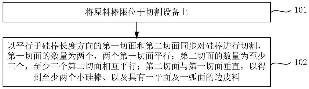
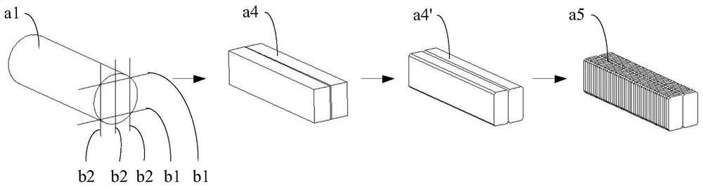
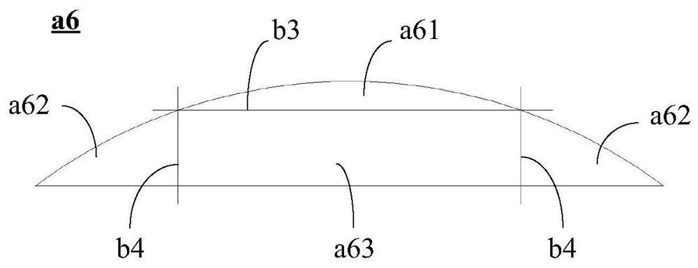
[0048] This embodiment provides a cutting device for silicon rods, which is used for cutting silicon rods to obtain small silicon chips. The silicon rod can be made of polycrystalline silicon material, single crystal silicon material, etc. In this embodiment, only single crystal silicon material is taken as an example to describe the cutting method in detail. Those skilled in the art can directly apply the technic...


PUM


Abstract

The embodiment of the invention provides silicon rod cutting equipment and system.The silicon rod cutting equipment comprises a base, a main rack, a bearing table and a linear cutting device; a cutting space is formed between a top plate of the main rack and the base; the bearing table is used for bearing silicon rods; the linear cutting device and the bearing table can slide relatively in the horizontal direction. The wire cutting device comprises two first cutting wire wheel sets and at least three second cutting wire wheel sets, cutting wires wound around the first cutting wire wheel sets are parallel to one another, and the wire cutting device is used for cutting the silicon rod along the first cutting face. The cutting lines wound on the second cutting line wheel sets are parallel to one another and used for cutting the silicon rod along the second tangent plane. The second tangent plane is perpendicular to the first tangent plane, and at least two small silicon rods with rectangular sections and edge materials are obtained. According to the silicon rod cutting equipment and system provided by the embodiment of the invention, the technical problem of cutting a small silicon wafer through a large silicon wafer in a traditional scheme can be solved.

Description

technical field [0001] The present application relates to hard and brittle material cutting technology, in particular to a silicon rod cutting equipment and system. Background technique [0002] With the development of heterojunction solar cells, the market demand for small silicon wafers is increasing, and the demand for thin wafers is also increasing. The thickness ranges from 180 microns to 150 microns. The future market may require 90 microns, or even 70 microns. , 80 micron thickness silicon wafer, and the thinner the silicon wafer, the smaller the silicon wafer specification is required to ensure the cutting quality and process. [0003] In the traditional solution, the small monocrystalline silicon cells are usually first cut into large silicon wafers from single crystal silicon rods, and then use laser technology to scribe and cut the large silicon wafers to form small silicon wafers, but in the process of laser scribing , will cause damage and defect states to the ...

Claims


Application Information

Patent Timeline
IPC IPC(8): B28D5/04B28D7/00B28D7/04B24B7/22B24B9/06
CPCB28D5/045B28D5/0064B28D5/0058B28D5/0082B28D5/0076B24B7/228B24B9/065
Inventor 王新辉周波戴鑫辉李林
Owner QINGDAO GAOCE TECH CO LTD
Why Eureka
Try Eureka