Method for cutting silicon rod through cross line, cutting equipment and cutting system

A reticle and cutting line cutting technology, applied in stone processing equipment, fine working devices, manufacturing tools, etc., can solve problems such as defects, small silicon wafer cross-section damage, and cutting difficulty, to ensure conversion efficiency, reduce Cutting steps, the effect of improving production efficiency

Pending Publication Date: 2022-06-21
QINGDAO GAOCE TECH CO LTD
View PDF0 Cites 0 Cited by
  • Summary
  • Abstract
  • Description
  • Claims
  • Application Information

AI Technical Summary

Problems solved by technology

The thickness of silicon wafers ranges from 180 microns to 150 microns, and the future market may even require 100 microns of silicon wafers. The thinner the silicon wafers, the more difficult it is to cut, and the less likely it is to guarantee the cutting quality.
[0003] In the traditional scheme, the cylindrical single crystal silicon rod is usually first cut into square rods, and then the square rods are cut into large silicon wafers, and then the large silicon wafers are diced and cut into small silicon wafers by laser technology. The scribing process will cause damage and defect states on the cross-section of the small silicon wafer, which will seriously affect the conversion efficiency of the final processed heterojunction cell

Method used


Image

  • Method for cutting silicon rod through cross line, cutting equipment and cutting system
  • Method for cutting silicon rod through cross line, cutting equipment and cutting system
  • Method for cutting silicon rod through cross line, cutting equipment and cutting system

Examples


Embodiment 1

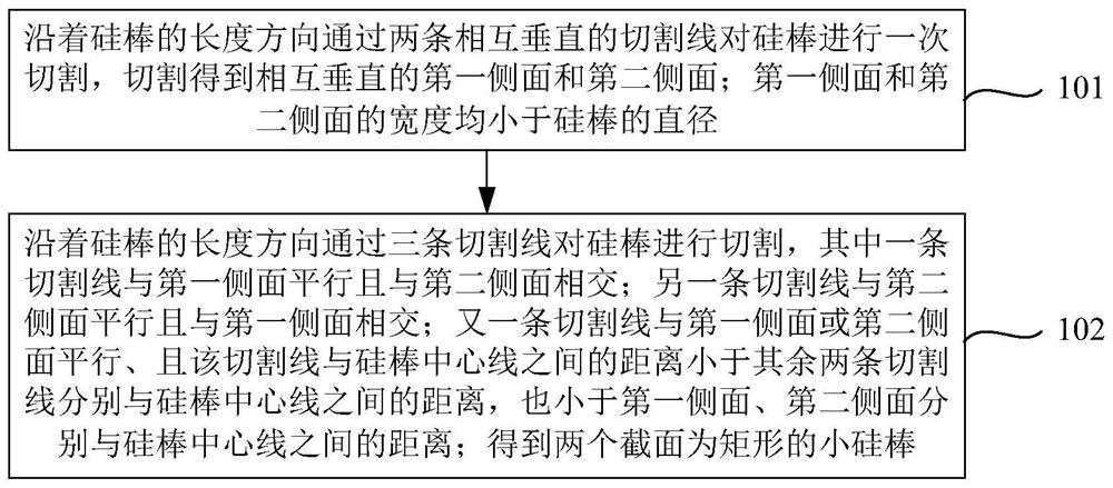
[0042] This embodiment provides a method for cutting a silicon rod with a cross line, which is used for cutting a single crystal silicon rod or a polycrystalline silicon rod. The cross section of the silicon rod can be circular, oval or irregular. This embodiment is described by taking a silicon rod with a circular cross section as an example. The silicon rod is cylindrical and has two circular end faces and a circumferential side surface located between the two end faces. The center line of the silicon rod passes through the two end faces. The center of the circle is perpendicular to the two end faces. The longitudinal direction of the silicon rod is a direction parallel to the center line of the silicon rod.

[0043] The silicon rod can be cut by cutting equipment such as a square cutter, and the cutting equipment is provided with a cutting line for cutting the silicon rod. Specifically, the cutting wire may be a diamond wire on which a plurality of fine-grained diamonds a...

Embodiment 2

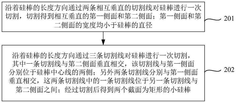
[0058] figure 2 The flow chart of the method for reticle cutting silicon rod provided in the second embodiment of the present application, image 3 This is a schematic structural diagram of the cross-cut silicon rod provided in the second embodiment of the present application. like figure 2 and image 3 As shown, the present embodiment provides a method for one-time cutting using three cutting lines, the method comprising:

[0059] In step 201, the silicon rod is cut once along the length direction of the silicon rod through two mutually perpendicular cutting lines to obtain mutually perpendicular first and second side surfaces; the widths of the first and second side surfaces are both smaller than those of the silicon rod. diameter of the rod.

[0060] The two cutting lines in this step are the first cutting line 51 and the second cutting line 52, the first cutting line 51 and the second cutting line 52 are perpendicular, and neither of them passes through the center li...

Embodiment 3

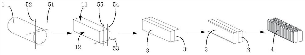
[0082] Based on the above embodiments, this embodiment provides a method for cutting a silicon rod with a cross line.

[0083] Figure 5 The flow chart of the method for reticle cutting silicon rod provided in the third embodiment of the present application, Image 6 This is a schematic structural diagram of the cross-cut silicon rod provided in the third embodiment of the present application. like Figure 5 and Image 6 As shown, the method for reticle cutting a silicon rod provided in this embodiment includes:

[0084] Step 301: Cut the silicon rod once along the length direction of the silicon rod through two mutually perpendicular cutting lines to obtain mutually perpendicular first side and second side; the widths of the first side and the second side are both smaller than diameter of the rod.

[0085] The two cutting lines in this step are the first cutting line 51 and the second cutting line 52, the first cutting line 51 and the second cutting line 52 are perpendic...


PUM

PropertyMeasurementUnit
thicknessaaaaaaaaaa

Abstract

The embodiment of the invention provides a method for cutting a silicon rod through a cross line, cutting equipment and a cutting system.The method comprises the steps that the silicon rod is cut once through two cutting lines perpendicular to each other in the length direction of the silicon rod, a first side face and a second side face are obtained through cutting, and the width of each side face is smaller than the diameter of the silicon rod; the silicon rod is cut through three cutting lines, and one cutting line is parallel to the first side face and intersects with the second side face; the other cutting line is parallel to the second side surface and intersects with the first side surface; another cutting line is parallel to the first side face or the second side face, and the distance between the cutting line and the center line of the silicon rod is smaller than the distance between the other two cutting lines and the center line of the silicon rod and is also smaller than the distance between the first side face and the center line of the silicon rod and the distance between the second side face and the center line of the silicon rod; and two small silicon rods with rectangular sections are obtained. According to the method for cutting the silicon rod through the cross line, the silicon rod with the small size can be directly obtained, and the silicon wafer is formed through slicing.

Description

technical field [0001] The present application relates to hard material cutting technology, and in particular, to a method, cutting equipment and cutting system for cutting silicon rods with cross-hairs. Background technique [0002] With the development of heterojunction cells, the demand for small silicon wafers is increasing, and the demand for thin wafers is also relatively large. The thickness of silicon wafers has increased from 180 microns to 150 microns. In the future, the market may even require silicon wafers with a thickness of 100 microns. The thinner the silicon wafer, the more difficult it is to cut, and the more difficult it is to guarantee the cutting quality. [0003] In the traditional scheme, the cylindrical monocrystalline silicon rod is usually cut into square rods, and then the square rod is cut into large silicon wafers, and then the large silicon wafers are diced and cut to form small silicon wafers using laser technology. The dicing process will cau...

Claims


Application Information

Patent Timeline
Patent Type & Authority Applications(China)
IPC IPC(8): B28D5/04B24B1/00
CPCB28D5/045B24B1/00
Inventor 周波范国强王叶兰于文文
Owner QINGDAO GAOCE TECH CO LTD
Why Eureka
Try Eureka