Preparation method of thin film transistor, thin film transistor and display device

A technology of thin-film transistors and masks, which is applied in the direction of transistors, semiconductor/solid-state device manufacturing, semiconductor devices, etc., can solve the problems of effective tail enlargement, achieve the effect of reducing tail, improving poor reliability, and improving product quality

Pending Publication Date: 2022-05-13
WUHAN BOE OPTOELECTRONICS TECH CO LTD +1
View PDF0 Cites 0 Cited by
  • Summary
  • Abstract
  • Description
  • Claims
  • Application Information

AI Technical Summary

Problems solved by technology

[0003] In view of this, an embodiment of the present invention provides a method for manufacturing a thin film transistor, a thin film transistor, and a display device, which solves the problem that the effective tail becomes larger during the channel fabrication process of the thin film transistor device

Method used


Image

  • Preparation method of thin film transistor, thin film transistor and display device
  • Preparation method of thin film transistor, thin film transistor and display device
  • Preparation method of thin film transistor, thin film transistor and display device

Examples


Embodiment Construction

[0041] The following will clearly and completely describe the technical solutions in the embodiments of the present invention with reference to the accompanying drawings in the embodiments of the present invention. Obviously, the described embodiments are only some of the embodiments of the present invention, not all of them. Based on the embodiments of the present invention, all other embodiments obtained by persons of ordinary skill in the art without creative efforts fall within the protection scope of the present invention.

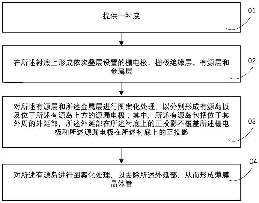
[0042] This embodiment provides a method for preparing a thin film transistor, such as figure 1 The preparation method of the thin film transistor shown includes:

[0043] Step 01: Provide a substrate 1 .

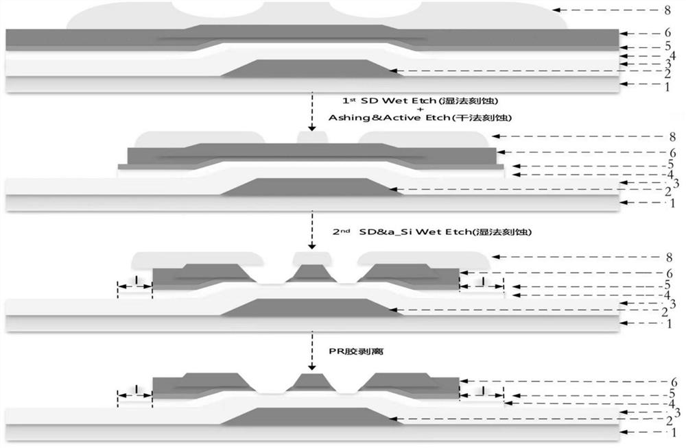
[0044] Step 02: Form a gate electrode 2, a gate insulating layer 3, an active layer 4 and a metal layer 6 sequentially stacked on the substrate 1.

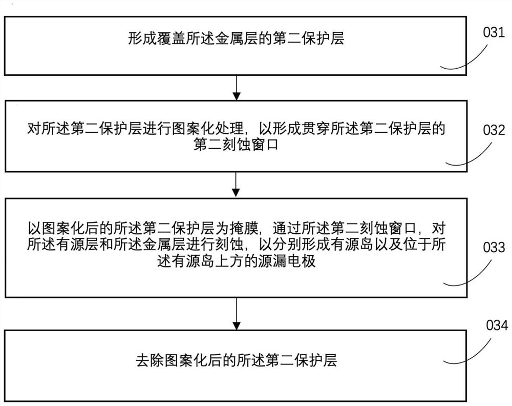
[0045] Step 03: Patterning the active layer 4 and the metal layer 6 to respectively form active i...


PUM


Abstract

The invention provides a preparation method of a thin film transistor, the thin film transistor and a display device. The problem that effective tail becomes large in the channel manufacturing process of a thin film transistor device is solved. The preparation method of the thin film transistor comprises the following steps: providing a substrate; forming a gate electrode, a gate insulating layer, an active layer and a metal layer which are sequentially laminated on the substrate; patterning the active layer and the metal layer to form an active island and source and drain electrodes located above the active island respectively; wherein the active island comprises an epitaxial part located on the periphery of the active island, and the orthographic projection of the epitaxial part on the substrate does not cover the orthographic projection of the gate electrode and the orthographic projection of the source and drain electrode on the substrate; and performing patterning processing on the active island to remove the epitaxial part so as to form the thin film transistor.

Description

technical field [0001] The invention relates to the field of display technology, in particular to a preparation method of a thin film transistor, a thin film transistor and a display device. Background technique [0002] At present, liquid crystal display (LCD, Liquid Crystal Display) is widely used in the fields of liquid crystal displays of various sizes due to its advantages of low power consumption, thin volume, wide viewing angle, and high definition. Usually, after the wet etching of the source / drain of the thin film transistor (TFT, ThinFilm Transistor) device, the ohmic contact layer and part of the dielectric layer are continuously etched to complete the channel fabrication of the thin film transistor device. The etching process is isotropic. During the etching process, the ohmic contact layer exposed to the etching solution will be completely removed, resulting in an increase in the effective tail and deterioration of the characteristics of the TFT device, such as ...

Claims


Application Information

Patent Timeline
IPC IPC(8): H01L21/336H01L29/786G02F1/1362G02F1/1368
CPCH01L29/66742H01L29/78609G02F1/1368G02F1/13625
Inventor 孔曾杰郭会斌高玉杰乔亚峥刘赫代耀丁俊陈鹏孙梦翔王谦
Owner WUHAN BOE OPTOELECTRONICS TECH CO LTD
Why Eureka
Try Eureka