Check patentability & draft patents in minutes with Patsnap Eureka AI!

Photodiode structure with dark current indication function and photoelectric sensor

A technology of photodiodes and photoelectric sensors, which is applied in the direction of transmitting sensing components, electric solid devices, circuits, etc. by using optical devices, can solve the problems of increasing the dark current of photodiodes and increasing noise, so as to improve photoelectric conversion efficiency, reduce noise, low cost effect

Pending Publication Date: 2022-05-13
NANO BEIJING PHOTONICS
View PDF0 Cites 0 Cited by
  • Summary
  • Abstract
  • Description
  • Claims
  • Application Information

AI Technical Summary

Problems solved by technology

During the entire receiving process, the photodiode’s ability to collect scattered signal light and photoelectric conversion efficiency are two key factors. In order to improve the above two performances, the most common solution in existing designs is to increase the aperture of the photodiode and the absorption layer. However, the larger the aperture and the thicker the absorbing layer will significantly increase the dark current of the photodiode, thereby increasing the noise

Method used


Image

  • Photodiode structure with dark current indication function and photoelectric sensor
  • Photodiode structure with dark current indication function and photoelectric sensor

Examples


Embodiment 1

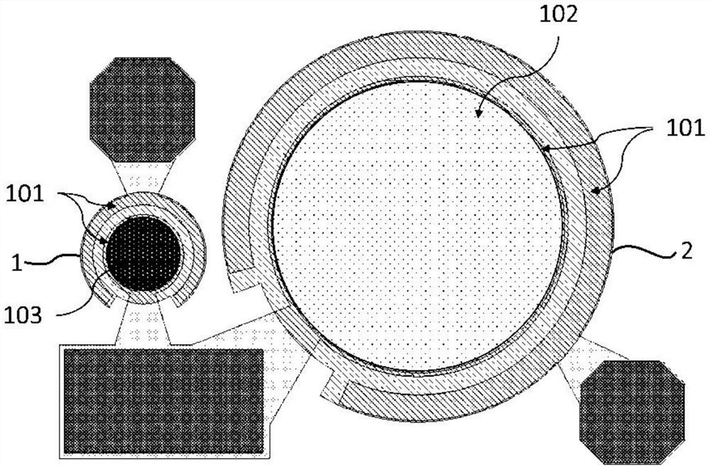
[0021] Such as Figure 1-2 As shown, the present invention provides a photodiode structure with a dark current indication function, including: a photosensitive photodiode 1 and a reference photodiode 2 .

[0022] The photosensitive photodiode 1 receives signal light through the photosensitive surface 102 and converts the light signal into an electrical signal.

[0023] The light-blocking layer 103 is provided on the photosensitive surface of the reference photodiode 2 , therefore, the reference photodiode 2 does not receive signal light, which is used to output a dark current reference value to indicate the dark current of the photosensitive photodiode 1 in real time. Wherein, the light-blocking layer 103 is a layer of material that is opaque in the diode working band, so that stray signal light cannot pass through at all, so as to ensure that the current output by the reference photodiode 2 at any time is its own dark current, so that Ensure that the dark current can be accu...

Embodiment 2

[0039] The present invention provides a photoelectric sensor, including: a processing module and the photodiode structure with dark current indication function in Embodiment 1.

[0040] The processing module is used to obtain two current signals output by the photosensitive photodiode 1 and the reference photodiode 2, and subtract the two current signals to eliminate dark current, and finally obtain an accurate signal photocurrent.

[0041] In practical application, the two sets of current signals output by the photodiode structure are collected by the external circuit at the same time, and input to the processing module for calculation. The processing module can be an arithmetic unit or a microcomputer processing system. The dark current Id of the photosensitive photodiode 1 感光 and the dark current Id of the reference photodiode 2 参考There is a fixed multiple relationship between: Id 感光 =N×Id 参考 .

[0042] There is a fixed multiplier relationship between the dark current o...


PUM


Abstract

The invention provides a photodiode structure with a dark current indication function. The photodiode structure comprises a photosensitive photodiode and a reference photodiode, the photosensitive surface of the reference photodiode is provided with a light blocking layer, and the dark current of the photosensitive photodiode and the dark current of the reference photodiode have a fixed multiple relationship. The invention further provides a photoelectric sensor which comprises a processing module and the photodiode structure. Through the structural design, the photodiode structure can output two paths of current signals, accurate incident light current can be obtained only by subtracting the two paths of current signals in actual work, the purposes of eliminating dark current and reducing noise are finally achieved, the dark current of the photodiode can be eliminated without additionally arranging a peripheral device, and the cost is reduced. Therefore, the solar cell has the advantages of simple structure and low cost, and the photoelectric conversion efficiency is further improved.

Description

technical field [0001] The invention belongs to the technical field of photoelectric detection equipment, and in particular relates to a photodiode structure and a photoelectric sensor with dark current indication function. Background technique [0002] As the core device of the photoelectric sensor, the photodiode can be used for distance detection, contact alarm and gesture recognition. In these applications, the photodiode receives the scattered signal light and converts the light signal into an electrical signal output. During the entire receiving process, the photodiode’s ability to collect scattered signal light and photoelectric conversion efficiency are two key factors. In order to improve the above two performances, the most common solution in existing designs is to increase the aperture of the photodiode and the absorption layer. However, the larger the aperture and the thicker the absorbing layer will significantly increase the dark current of the photodiode, ther...

Claims


Application Information

Patent Timeline
IPC IPC(8): H01L25/04G01D5/34H01L31/02H01L31/0224
CPCG01D5/34H01L25/042H01L31/02019H01L31/022408G01J1/4228G01J2001/446H01L31/02027G01J1/44H01L31/02164H01L31/028H01L31/1075
Inventor 石彬祁帆蔡鹏飞
Owner NANO BEIJING PHOTONICS
Features
  • R&D
  • Intellectual Property
  • Life Sciences
  • Materials
  • Tech Scout
  • Unparalleled Data Quality
  • Higher Quality Content
  • 60% Fewer Hallucinations
Learn More