Pattern reconfigurable phase bit antenna and two-dimensional beam scanning array thereof
A pattern and phase technology, applied to antenna arrays, individually powered antenna arrays, antennas, etc., can solve the problems of large-scale array elements and large occupied space, difficulty in wide-angle scanning, and difficulty in one-dimensional linear arrays. The effect of large-scale array and regular array, high radiation performance and low cost
- Summary
- Abstract
- Description
- Claims
- Application Information
AI Technical Summary
Problems solved by technology
Method used
Image

Examples
Embodiment 1
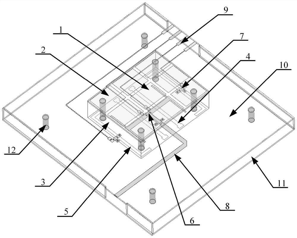
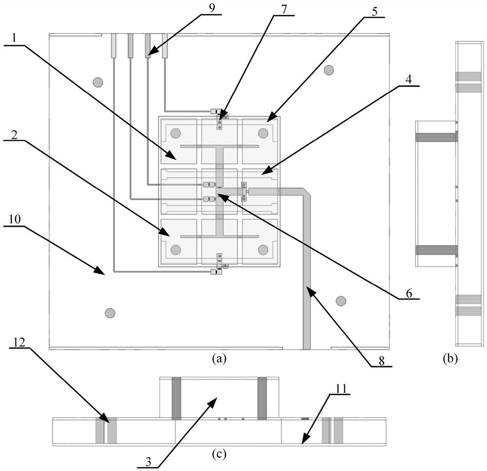
[0038] Such as Figure 1-Figure 2 As shown, the present invention provides a pattern reconfigurable phase bit antenna, including a miniaturized electromagnetic metasurface 1, a metal patch unit 2, a dielectric resonator 3, a phase 1 bit coupling feeding slot 4, and a reflector radiation slot 5. Phase bit switch circuit 6, reconfigurable reflector gap switch circuit 7, feed microstrip line 8, switch DC bias circuit 9, metal floor 10, metal reflector 11 and nylon screw 12;
[0039] The miniaturized electromagnetic metasurface 1 is composed of a metal patch unit 2 and a dielectric resonator 3, wherein the metal patch unit 2 on the miniaturized electromagnetic metasurface 1 is a small periodic metal patch attached to a dielectric resonator The upper surface of the resonator 3, the dielectric resonator 3 is a dielectric material with high dielectric constant and low loss, the dielectric resonator 3 is fixed on the metal floor 10 through the nylon screw 12, and the phase 1 bit The ...
Embodiment 2
[0044] Such as Figure 5 and Figure 6 As shown, the present invention provides a two-dimensional beam scanning array based on a one-dimensional linear array, including the reconfigurable phase 1-bit antenna of the pattern described in Embodiment 1 and several antenna elements 13; the several antennas The array element 13 is composed of the 1-bit antenna with a reconfigurable phase of the pattern as an array element, and each antenna array element 13 is arranged in a linear and equidistant manner.
[0045] In this embodiment, four antenna elements (C1-C4) are taken as an example for illustration.
[0046]In this embodiment, a digital multi-beam array based on a one-dimensional linear array and two-dimensional scanning provided by the present invention includes a miniaturized electromagnetic metasurface 1, a metal patch unit 2, a dielectric resonator 3, and a phase 1-bit coupling feed slot 4 , reflector radiation gap 5, phase bit switch circuit 6, reconfigurable reflector gap...
PUM
 Abstract
Description
Claims
Application Information
 - R&D
- Intellectual Property
- Life Sciences
- Materials
- Tech Scout
- Unparalleled Data Quality
- Higher Quality Content
- 60% Fewer Hallucinations
Browse by: Latest US Patents, China's latest patents, Technical Efficacy Thesaurus, Application Domain, Technology Topic, Popular Technical Reports.
© 2025 PatSnap. All rights reserved.Legal|Privacy policy|Modern Slavery Act Transparency Statement|Sitemap|About US| Contact US: help@patsnap.com