Signal pin set device

A technology of signal pins and pins, which is applied in the direction of coupling devices, parts of connection devices, electrical components, etc., can solve problems such as occupancy, inability to achieve full shielding, and multiple PCB spaces, so as to ensure full isolation and meet signal requirements. Wiring requirements, rational use of improved effects

Active Publication Date: 2022-05-13
INSPUR SUZHOU INTELLIGENT TECH CO LTD
View PDF1 Cites 0 Cited by
  • Summary
  • Abstract
  • Description
  • Claims
  • Application Information

AI Technical Summary

Problems solved by technology

[0005] The defect exposed by this existing signal pin arrangement scheme is that the high-speed signal pins are only provided with ground pins on both sides, which cannot be completely shielded; It will take up more PCB space when wiring

Method used


Image

  • Signal pin set device
  • Signal pin set device
  • Signal pin set device

Examples


Embodiment 1

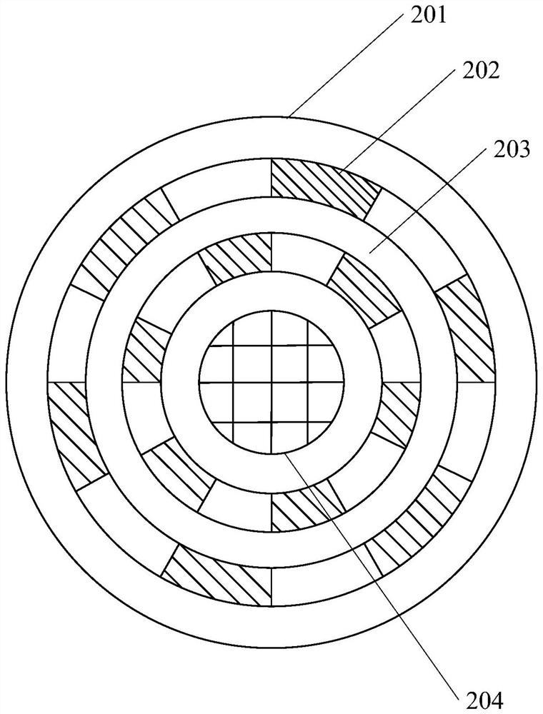
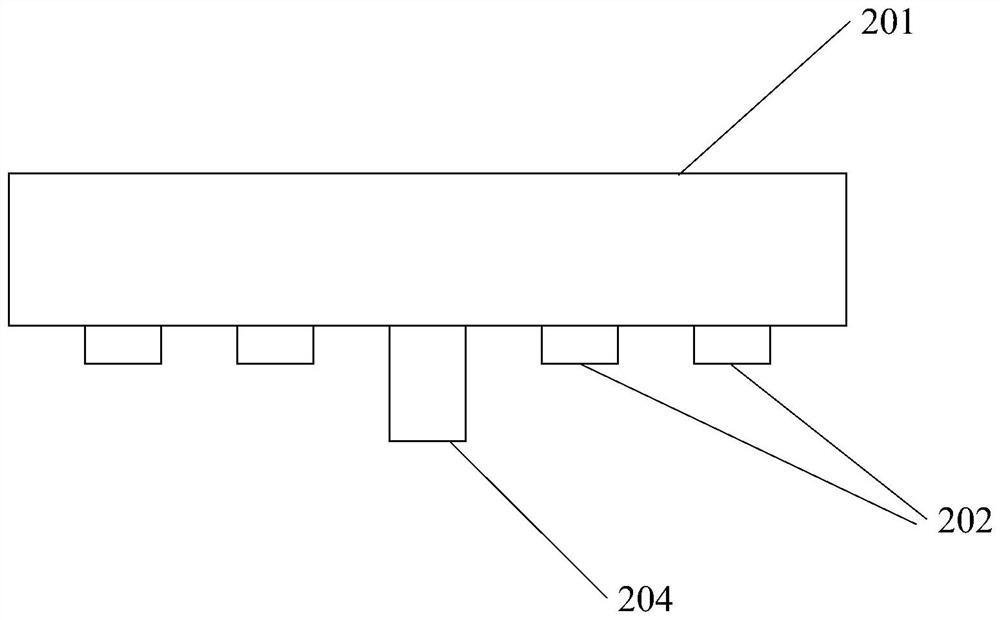
[0028] figure 2 A schematic plan view of a signal pin set device provided in an embodiment of the present application; image 3 It is a schematic side view of a signal pin set device provided in an embodiment of the present application.

[0029] Such as figure 2 As shown, the signal pin set device provided by the embodiment of the present application includes: a device body 201, a plurality of conductor materials 202 arranged on the device body 201, each conductor material 202 is filled with an insulating material 203, and each conductor material 202 is filled with an insulating material 203. Both have signal pins and ground pins;

[0030] Wherein, the arrangement position of each conductor material 202 is determined according to the size of the available space of the signal pin set device and the shape of the available space of the signal pin set device.

[0031] It should be noted, figure 2 The area shaded by the oblique line is the conductor material 202 , and the wh...

Embodiment 2

[0041] On the basis of the above-mentioned embodiments, in the signal pin set device provided by the embodiment of the present application, in order to further optimize the layout effect, improve the space utilization rate and strengthen the signal shielding effect, the device body 201 can adopt such as figure 2 with image 3 In the illustrated cylindrical structure, the conductive material 202 is arranged on the circular face of the cylindrical structure. Of course, while the conductor material 202 is arranged in a concentric circle structure, the device body 201 is not limited to a cylindrical structure, and may also be other three-dimensional structures.

[0042] then as figure 2 As shown, each conductor material 202 can be arranged in a concentric circle structure on the device body 201, and an insulating material ring is filled between two adjacent conductor material rings. which is figure 2 The ring where the hatching of the oblique line is located is the conductor m...

Embodiment 3

[0048] On the basis of the above-mentioned embodiments, the signal pin set device provided in the embodiment of the present application may further include ground vias disposed between adjacent conductive materials 202 .

[0049] When designing for high-speed signals, the signal pin set device provided by the embodiment of the present application can provide ground vias between adjacent conductor materials 202 for backflow and signal interference shielding to ensure signal integrity.

[0050] If used as figure 2 In the layout of the conductor material 202 shown, grounding vias can be provided between adjacent conductor material rings and between signal pins on the same conductor material ring.

[0051] The signal pin assembly device provided by the embodiment of the present application, for high-speed signals, provides ground vias between adjacent conductor materials for backflow and shielding signal interference, and further optimizes signal integrity on the basis of the abo...


PUM


Abstract

The invention discloses a signal pin set device which is composed of a device body and a plurality of conductor materials arranged on the device body, and the arrangement positions of the conductor materials are flexibly arranged according to the size and the shape of an available space instead of an existing mode that the conductor materials are fixedly arranged on one conductor material in a linear mode. Therefore, the signal shielding level is improved while the reasonable utilization of the layout space is ensured; each conductor material is provided with a signal pin and a grounding pin, so that the signal wiring requirement is met; insulating materials are filled among the conductor materials, so that signal isolation among the conductor materials is realized. One or more signal pins can be arranged on one conductor material according to the requirement of signals on the shielding effect and different signal types, for example, one high-speed signal pin independently occupies one conductor material, and comprehensive isolation of high-speed signals is guaranteed.

Description

technical field [0001] The present application relates to the field of electronic equipment, in particular to a signal pin set device. Background technique [0002] With the rapid development of the server industry, the functions to be implemented by server boards are increasing, the signal rate is getting higher and higher, and the density of boards is increasing. In the limited space of the board (also printed circuit board, Printed Circuit Board, PCB), to achieve more functions and ensure the integrity of high-speed signals is the current challenge for hardware development. [0003] figure 1 It is a schematic diagram of pin arrangement of an existing electronic component. [0004] Such as figure 1 As shown, in the existing signal pin arrangement scheme, most of the pins are arranged in a straight line, including ground pins 101 , high-speed signal pins 102 , single-ended signal pins 106 and so on. When high-speed signal pins 102 exist, ground pins 101 need to be added...

Claims


Application Information

Patent Timeline
Patent Type & Authority Applications(China)
IPC IPC(8): H01R13/6471H01R13/6594
CPCH01R13/6471H01R13/6594
Inventor 王英娜周冬
Owner INSPUR SUZHOU INTELLIGENT TECH CO LTD
Why Eureka
Try Eureka