Automatic surface mounting equipment for electronic components

A technology for electronic components and chip components, which is applied in the field of automatic chip mounting equipment for electronic components, can solve the problems of too much solder paste on circuit boards and cumbersome solder paste coating operations on circuit boards, etc. The effect of bending damage and convenient cutting

Active Publication Date: 2022-05-13
华研电子科技(徐州)有限公司
View PDF4 Cites 6 Cited by
  • Summary
  • Abstract
  • Description
  • Claims
  • Application Information

AI Technical Summary

Problems solved by technology

[0003] The currently used automatic placement equipment for electronic components needs to apply solder paste on the circuit board and then attach the chip components to the circuit board during the placement process, and such electronic components automatic placement process There are the following problems: the solder paste coated on the circuit board is difficult to accurately coat according to the size of the chip components, resulting in more or less solder paste on the circuit board. When the position changes, the solder paste application position also changes at the same time, which causes the problem of cumbersome solder paste application on the circuit board

Method used


Image

  • Automatic surface mounting equipment for electronic components
  • Automatic surface mounting equipment for electronic components
  • Automatic surface mounting equipment for electronic components

Examples


Embodiment Construction

[0031] The embodiments of the present invention will be described in detail below with reference to the accompanying drawings, but the present invention can be implemented in many different ways defined and covered by the claims.

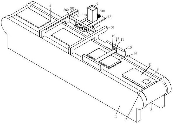
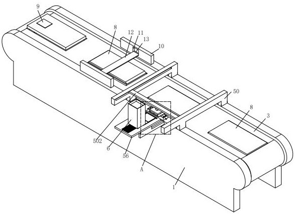
[0032] refer to figure 1 and Figure 4 , an electronic component automatic chip placement equipment, including a support frame 1, a rotating shaft 2, a conveyor belt 3 and a fixing groove 4, the two support frames 1 are symmetrically arranged front and back, and the gap between the two support frames 1 Rotationally connected with rotating shafts 2 symmetrically arranged left and right. The two rotating shafts 2 are connected by a conveyor belt 3. The conveyor belt 3 is provided with fixing grooves 4 arranged along its circumference, and circuit boards are placed in the fixing grooves 4. 8. A patch mechanism 5 is installed on the upper end surfaces of the two supporting frames 1, and a storage tube 6 for storing patch components 9 is installed on th...


PUM


Abstract

The invention relates to the technical field of electronic component surface mounting, in particular to electronic component automatic surface mounting equipment which comprises a supporting and fixing frame, a rotating shaft, a conveying belt and a fixing groove. According to the automatic surface mounting equipment for the electronic component, the surface mounting mechanism is adopted to coat the surface mounting component with the solder paste, and then the surface mounting component is mounted on a circuit board by adjusting the position of the surface mounting component; the problem that the solder paste on the circuit board is too much or little due to the fact that the solder paste coated on the circuit board is difficult to accurately coat according to the size of the patch component is solved, meanwhile, the solder paste is directly coated on the patch component, only the patch position of the patch component needs to be adjusted, and the production efficiency is improved. And the problem that the surface mounting of the electronic component is relatively tedious due to the fact that the tin paste coating position and the surface mounting component position are all adjusted is avoided.

Description

technical field [0001] The invention relates to the technical field of electronic component placement, in particular to an electronic component automatic placement equipment. Background technique [0002] The basic process of chip components is: solder paste printing, parts mounting, reflow soldering, AOI optical inspection, maintenance, board splitting, etc. Among them, automatic chip placement equipment for electronic components is required in the part mounting step. Automatic placement equipment for electronic components refers to a kind of equipment that accurately attaches chip components to circuit boards coated with solder paste, which can effectively improve the efficiency of placement. [0003] The currently used automatic placement equipment for electronic components needs to apply solder paste on the circuit board and then attach the chip components to the circuit board during the placement process, and such electronic components automatic placement process There...

Claims


Application Information

Patent Timeline
Patent Type & Authority Applications(China)
IPC IPC(8): H05K3/34H05K13/00
CPCH05K3/341H05K3/3494H05K13/00H05K13/0061
Inventor 吴升堂
Owner 华研电子科技(徐州)有限公司
Why Eureka
Try Eureka