Cold source Schottky transistor and preparation process thereof

A preparation process and transistor technology, which is applied in semiconductor/solid-state device manufacturing, semiconductor devices, electrical components, etc., can solve the problems that the sub-threshold swing cannot be broken through, and the power supply voltage and power consumption of MOSFET devices cannot be further reduced.

Pending Publication Date: 2022-05-17
PEKING UNIV
View PDF0 Cites 1 Cited by
  • Summary
  • Abstract
  • Description
  • Claims
  • Application Information

AI Technical Summary

Problems solved by technology

[0003] The invention provides a cold-source Schottky transistor and its preparation process, which is used to solve the defect that the sub-threshold swing of the MOSFET in the prior art cannot break through 60mV / dec, so that the power supply voltage and power consumption of the MOSFET device cannot be further reduced.

Method used


Image

  • Cold source Schottky transistor and preparation process thereof
  • Cold source Schottky transistor and preparation process thereof
  • Cold source Schottky transistor and preparation process thereof

Examples


Embodiment Construction

[0097] In order to make the purpose, technical solutions and advantages of the present invention clearer, the technical solutions in the present invention will be clearly and completely described below in conjunction with the accompanying drawings in the present invention. Obviously, the described embodiments are part of the embodiments of the present invention , but not all examples. Based on the embodiments of the present invention, all other embodiments obtained by persons of ordinary skill in the art without creative efforts fall within the protection scope of the present invention.

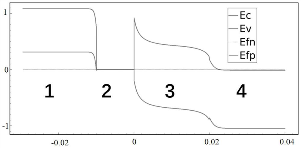
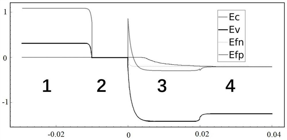
[0098] Combine below Figure 1 to Figure 78 The cold source Schottky transistor of the present invention and its preparation process are described.

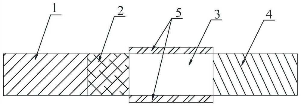
[0099] Such as figure 1 As shown, a cold source Schottky transistor provided by the present invention includes a substrate 101, a source region, a drain region 4, a channel region 3, a source, a drain and a gate.

[0100] Specifically, the so...


PUM

PropertyMeasurementUnit
thicknessaaaaaaaaaa
lengthaaaaaaaaaa
electron work functionaaaaaaaaaa

Abstract

The invention provides a cold source Schottky transistor and a preparation process thereof. The cold source Schottky transistor comprises a substrate, a source region, a channel region, a source electrode, a drain electrode and a grid electrode, the source region is arranged on the substrate and comprises a first source region and a metal region connected with the first source region, and the first source region is a heavily doped region; the drain region is arranged on the substrate, the drain region is a heavily doped region, and the doping type of the drain region is opposite to that of the first source region; the channel region is arranged on the substrate, the channel region is located between the metal region and the drain region, and the upper side and / or the lower side of the channel region are / is provided with a gate dielectric; the source electrode is arranged on the source region; the drain electrode is arranged on the drain region; the grid electrode is arranged on the grid electrode medium. Under the condition of certain source-drain bias voltage, in the process of increasing the gate voltage, the Schottky barrier between the channel region and the metal region is lowered, the Schottky barrier is thinned until the Schottky barrier of the low-energy region is thin enough, the tunneling current is increased rapidly, electrons of the low-energy region of the source region tunnel the Schottky barrier, and the tunneling current is increased rapidly. Therefore, the subthreshold swing can be lower than 60mV / dec.

Description

technical field [0001] The invention relates to the technical field of semiconductors, in particular to a cold source Schottky transistor and a preparation process thereof. Background technique [0002] The miniaturization of metal-oxide-semiconductor field-effect transistors (MOSFETs) under Moore's Law has led to the continuous development of information technology over the past few decades. By reducing the channel length of transistors, switching speeds have become faster, device densities have become higher, and circuits become more powerful and efficient. However, the exponential increase in device performance cannot continue forever as predicted by Moore's Law. Among the problems faced by transistor technology today, power consumption is a prominent issue due to the limitation of reduction in supply voltage. Especially under the limitation of the device principle of MOSFET, no matter what kind of channel material and device structure are used, the limit of the sub-thre...

Claims


Application Information

Patent Timeline
Patent Type & Authority Applications(China)
IPC IPC(8): H01L29/78H01L21/336
CPCH01L29/66643H01L29/7839
Inventor 刘飞谢晓鑫刘晓彦康晋锋
Owner PEKING UNIV
Why Eureka
Try Eureka