
Package with polymer pillars and raised portions

A package, polymer technology, applied in the direction of semiconductor/solid state device components, electrical components, semiconductor devices, etc., can solve problems such as reducing the availability of electronic equipment, WLCSP not operating normally or as expected, solder ball crosstalk, etc.

Pending Publication Date: 2022-05-20
STMICROELECTRONICS SRL
View PDF0 Cites 0 Cited by
  • Summary
  • Abstract
  • Description
  • Claims
  • Application Information

AI Technical Summary

Problems solved by technology

For example, if during the reflow process of mounting a WLCSP to a PCB with solder balls, the solder balls can physically touch each other, or can come close enough to each other to cause arcing, which can cause crosstalk between adjacent solder balls, causing the WLCSP to malfunction or run as expected
Such inappropriate functionality may significantly reduce the usability of an electronic device as a whole, be it a telephone, smartphone, tablet, television, computer, notebook, camera, or some other electronic device in which the semiconductor package resides

Method used


Image

  • Package with polymer pillars and raised portions
  • Package with polymer pillars and raised portions
  • Package with polymer pillars and raised portions

Examples


Embodiment Construction

[0029] In the following description, certain specific details are set forth in order to provide a thorough understanding of various embodiments of the present disclosure. However, it will be understood by those skilled in the art that the present disclosure may be practiced without these specific details. In other instances, well-known structures associated with electronic components, packages, and semiconductor manufacturing techniques have not been described in detail to avoid unnecessarily obscuring the description of the embodiments of the present disclosure.

[0030] Throughout the specification and the following claims, unless the context requires otherwise, the word "comprise" and variations thereof, such as "comprises" and "comprising", shall be used with the open, Inclusive to explain, that is, "including but not limited to (including, but not limited to)".

[0031] The use of first, second, third, etc. ordinal numbers does not necessarily imply a sense of order, but...


PUM


Abstract

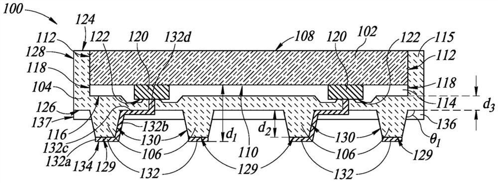
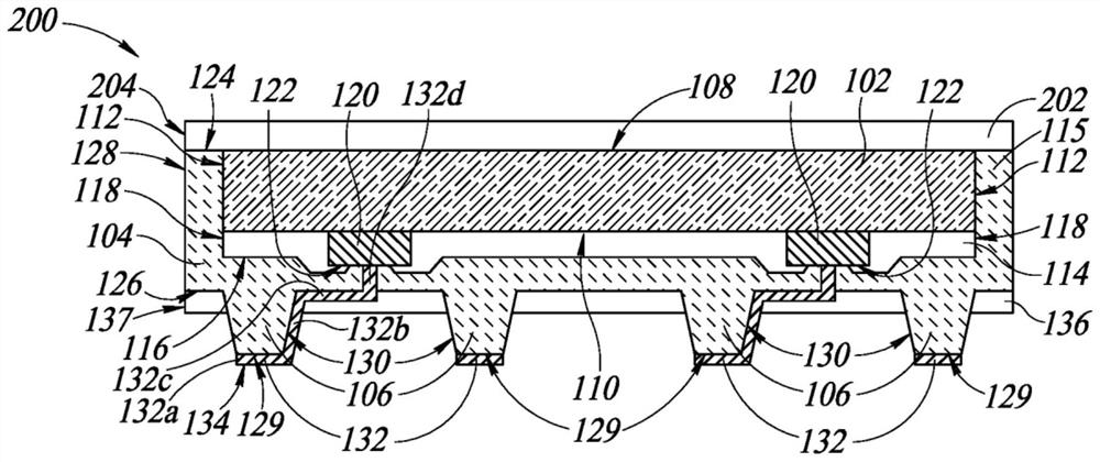
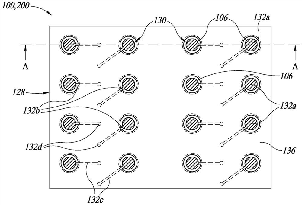
Embodiments of the present disclosure relate to packages having polymer pillars and raised portions. The present disclosure relates to a semiconductor package including a molding compound having at least one raised portion extending outwardly from the package. In some embodiments, the semiconductor package has a plurality of raised portions, and a plurality of conductive layers on the plurality of raised portions. The plurality of raised portions and the plurality of conductive layers are used to mount the semiconductor package to an external electronic device (e.g., a printed circuit board (PCB), another semiconductor package, an external electrical connection, etc. In some embodiments, the semiconductor package has a single raised portion with a plurality of conductive layers on the single raised portion. The semiconductor package is mounted onto an external electronic device using a single raised portion and a plurality of conductive layers. The plurality of conductive layers on the plurality of raised portions or a single raised portion may be formed by a laser direct structuring (LDS) process.

Description

technical field [0001] The present disclosure relates to packages having polymers that include posts or raised portions. Background technique [0002] In general, a semiconductor device package, such as a chip-scale package or wafer-level chip-scale package (WLCSP), contains a semiconductor device, semiconductor die, or integrated circuit packaged in a molding compound, polymer, encapsulant, or the like die. A semiconductor device, semiconductor die, or integrated circuit die may be a sensor configured to detect any quantity or quality, or may be a controller for controlling various other electronic components. For example, such semiconductor device packages may detect light, temperature, sound, pressure, stress, strain, or any other quantity or quality. The other semiconductor device, semiconductor die or integrated circuit die may be a controller, microprocessor, memory or some other type of semiconductor device, semiconductor die or integrated circuit die. [0003] Con...

Claims


Application Information

Patent Timeline
Patent Type & Authority Applications(China)
IPC IPC(8): H01L23/31H01L23/48H01L21/56H01L21/60H01L23/488
CPCH01L23/3128H01L23/481H01L24/11H01L24/13H01L24/02H01L21/56H01L2224/02331H01L2224/02333H01L2224/02373H01L2224/02381H01L2224/02379H01L2224/111H01L2224/13009H01L2924/1815H01L2224/12105H01L2224/04105H01L2924/18162H01L21/6835H01L2221/6834H01L2221/68327H01L21/6836H01L23/3114H01L21/561H01L2224/94H01L2224/96H01L2224/0231H01L24/96H01L24/94H01L2224/0235H01L2224/0236H01L2224/05548H01L2224/13024H01L2224/05647H01L2224/05655H01L2224/05639H01L2224/0239H01L2224/056H01L2224/131H01L2224/05644H01L2224/03H01L2224/02H01L2224/11H01L2924/00014H01L2924/013H01L2924/01029H01L2924/01028H01L2924/01047H01L2924/01079H01L2924/014H01L24/20H01L24/19H01L2224/2105H01L2224/2101
Inventor 栾竟恩
Owner STMICROELECTRONICS SRL
Learn More