Vertical transistor, display pixel, vertical light-emitting transistor and display panel

A light-emitting transistor, vertical technology, applied in semiconductor devices, electrical solid state devices, semiconductor/solid state device manufacturing, etc., can solve problems such as working current adjustment, low device performance, and inability to reduce working voltage, so as to reduce working voltage and device good performance

Pending Publication Date: 2022-05-27
BOE TECH GRP CO LTD
View PDF0 Cites 0 Cited by
  • Summary
  • Abstract
  • Description
  • Claims
  • Application Information

AI Technical Summary

Problems solved by technology

[0004] In view of this, the embodiments of the present disclosure propose a vertical transistor, a display pixel, a vertical light-emitting transistor, and a display panel to solve the following problems in the prior art: the exi

Method used


Image

  • Vertical transistor, display pixel, vertical light-emitting transistor and display panel
  • Vertical transistor, display pixel, vertical light-emitting transistor and display panel
  • Vertical transistor, display pixel, vertical light-emitting transistor and display panel

Examples


Example Embodiment

[0042] Example 1

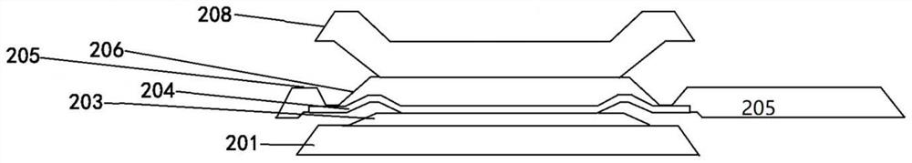
[0043] The present disclosure embodiment provides a display pixel, wherein the cross-sectional structure is illustrated as Figure 7 shown, at least includes:

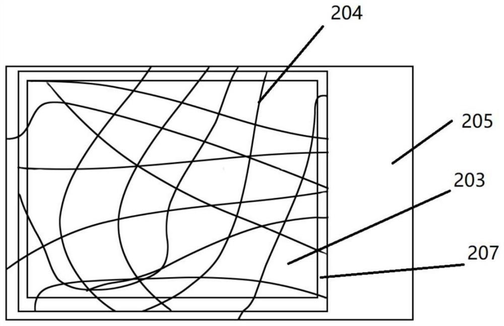
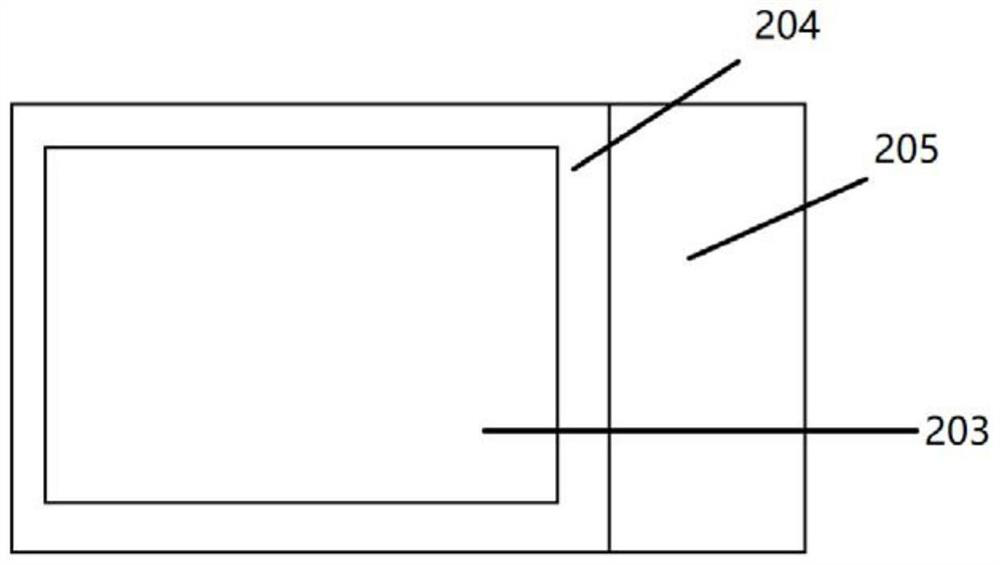
[0044] Source layer 201, gate layer, drain layer 208, first active layer 203, second active layer 206; source layer, first active layer, gate layer, second active layer, drain layer in the vertical direction of stacking settings, gate layer includes the first gate structure 204 and the second gate structure 205, the first active layer, the second active layer and the first gate structure to form a Schottky contact, vertical direction is perpendicular to the direction of the substrate; the first gate structure is located in the vertical stacking connection area, There is a first active overlapping region with the source layer in the vertical direction, and there is a second active overlapping region with the gate layer in the vertical direction, the first gate structure adopts a sparse gate material or has...

Example Embodiment

[0049] Example 2

[0050] The present disclosure embodiment also provides a pixel circuit, the cross-sectional structure of which is illustrated as Figure 8 as shown, relative to Figure 7 As far as the pixel circuit shown, the basic structure of the source layer 201, gate layer, drain layer 208, the first active layer 203, the second active layer 206 remains unchanged, i.e., at least comprising:

[0051] Source layer 201, gate layer, drain layer 208, first active layer 203, second active layer 206; source layer, first active layer, gate layer, second active layer, drain layer in the vertical direction of stacking settings, gate layer includes the first gate structure 204 and the second gate structure 205, the first active layer, the second active layer and the first gate structure to form a Schottky contact, vertical direction is perpendicular to the direction of the substrate; the first gate structure is located in the vertical stacking connection area, There is a first active ov...

Example Embodiment

[0054] Example 3

[0055] The present embodiment of the present disclosure also provides a vertical type light emitting transistor, the profile structure of which is illustrated as shown Figure 9 (emits light through the drain layer, so in the image looks equivalent to omitting the drain layer) as shown, including at least:

[0056] Source layer 201, gate layer, drain layer 208, first active layer 203, second active layer 206; source layer, first active layer, gate layer, second active layer, drain layer in the vertical direction of stacking settings, gate layer includes the first gate structure 204 and the second gate structure 205, the first active layer, the second active layer and the first gate structure to form a Schottky contact, vertical direction is perpendicular to the direction of the substrate; the first gate structure is located in the vertical stacking connection area, There is a first active overlapping region with the source layer in the vertical direction, and the...


PUM


Abstract

The embodiment of the invention provides a vertical transistor, a display pixel, a vertical light-emitting transistor and a display panel, the vertical transistor comprises a source electrode layer, a first active layer, a grid electrode layer, a second active layer and a drain electrode layer which are sequentially stacked in the vertical direction, and the grid electrode layer comprises a first grid electrode structure and a second grid electrode structure, the first active layer and the second active layer form Schottky contact with the first gate structure; the first gate structure is located in the vertical stacking connection region, a first active overlapping region exists between the first gate structure and the source layer in the vertical direction, a second active overlapping region exists between the first gate structure and the gate layer in the vertical direction, and the first gate structure adopts a sparse gate material or has a sparse hollow structure; the first active overlapping region is a projection overlapping part of two connecting surfaces for connecting the first active layer with the source electrode layer and the grid electrode layer, and the second active overlapping region is a projection overlapping part of two connecting surfaces for connecting the second active layer with the drain electrode layer and the grid electrode layer; the second gate structure is located in the non-vertical stack connection region.

Description

Technical field [0001] The present disclosure relates to the field of display and control, in particular to a vertical transistor, display pixels, vertical light-emitting transistors and display panels. Background [0002] A gate-source-drain vertical distribution of gate-source-drain Vertical Field Effect Transistor (referred to as VOFET) structure, which is a flat plate capacitor unit superimposed active layer and drain electrode, which can reduce the distance between the source drain (active layer deposition thickness is the length of the channel), increase the area of the conductive channel between the source drain, Solve the problem of higher working voltage and small working current caused by excessive resistance of organic semiconductor transistors with airport effect. [0003] However, the depth of the channel is controlled by the gate, which can usually only stay a few nanometers, can not be more adjusted at the same voltage to the operating current, can not be further r...

Claims


Application Information

Patent Timeline
IPC IPC(8): H01L51/52H01L27/32H01L51/05H01L51/10
CPCH10K59/1213H10K10/491H10K10/464H10K10/82H10K50/805H10K50/30
Inventor 宋尊庆
Owner BOE TECH GRP CO LTD
Why Eureka
Try Eureka