Unlock instant, AI-driven research and patent intelligence for your innovation.

Three-dimensional memory devices, systems, and methods of forming same

A memory and equipment technology, applied in semiconductor devices, electric solid state devices, electrical components, etc., can solve the problem of high cost

Pending Publication Date: 2022-05-27
YANGTZE MEMORY TECH CO LTD
View PDF0 Cites 0 Cited by
  • Summary
  • Abstract
  • Description
  • Claims
  • Application Information

AI Technical Summary

Problems solved by technology

However, as the feature size of memory cells approaches the lower limit, planar processes and fabrication techniques become challenging and costly
As a result, the storage density of planar memory cells approaches the upper limit

Method used


Image

  • Three-dimensional memory devices, systems, and methods of forming same
  • Three-dimensional memory devices, systems, and methods of forming same
  • Three-dimensional memory devices, systems, and methods of forming same

Examples


Embodiment Construction

[0039] While specific configurations and arrangements are discussed, it should be understood that this is done for illustrative purposes only. Accordingly, other configurations and arrangements may be used without departing from the scope of the present disclosure. In addition, the present disclosure may also be used in various other applications. Functional and structural features as described in this disclosure may be combined, adapted, and modified with each other and in ways not specifically shown in the accompanying drawings, such that such combinations, adaptations, and modifications are within the scope of this disclosure.

[0040] Generally, terms can be understood, at least in part, from their contextual usage. For example, the term "one or more" as used herein may be used in the singular to describe any feature, structure or characteristic or may be used in the plural to describe a combination of features, structures or characteristics, depending at least in part on...


PUM


Abstract

A three-dimensional (3D) memory device includes a first semiconductor structure and a second semiconductor structure. The first semiconductor structure includes a first semiconductor layer and an NAND memory string array. The second semiconductor structure is under the second side of the first semiconductor layer. The second side of the first semiconductor layer is opposite the first side of the first semiconductor layer. The second semiconductor structure includes a second semiconductor layer, a first peripheral circuit, and a second peripheral circuit. The first peripheral circuit includes a first transistor in contact with a first side of the second semiconductor layer. The second peripheral circuit includes a second transistor in contact with a second side of the second semiconductor layer. The second side of the second semiconductor layer is opposite the first side of the second semiconductor layer.

Description

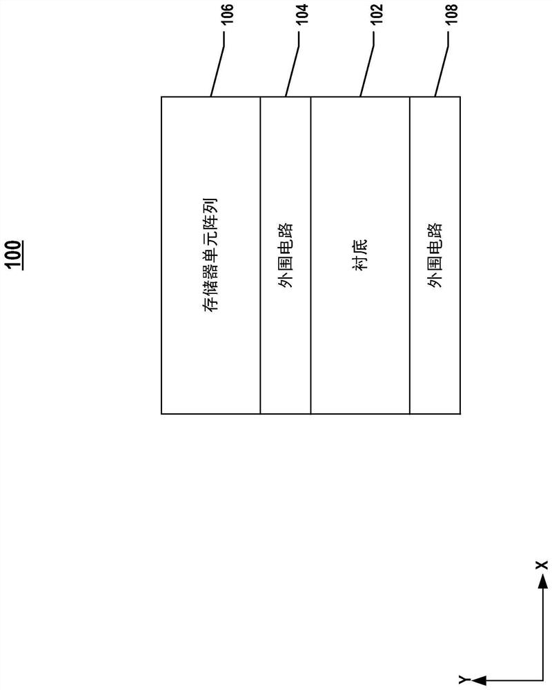
[0001] CROSS-REFERENCE TO RELATED APPLICATIONS [0002] This application claims the benefit of priority to International Application No. PCT / CN2021 / 103762, filed June 30, 2021, the entire contents of which are incorporated herein by reference. technical field [0003] The present disclosure relates to memory devices and methods of fabricating the same, and in particular, to three-dimensional (3D) memory devices and methods of fabricating the same. Background technique [0004] Shrinking planar memory cells to smaller sizes through improvements in process technology, circuit design, programming algorithms, and manufacturing processes. However, as the feature size of memory cells approaches the lower limit, planar processes and fabrication techniques become challenging and costly. As a result, the storage density of planar memory cells is approaching an upper limit. [0005] 3D memory architectures can address density constraints in planar memory cells. A 3D memory architec...

Claims


Application Information

Patent Timeline
IPC IPC(8): H01L27/11573H01L27/11575H01L27/11582H01L27/1157
CPCH10B43/35H10B43/50H10B43/40H10B43/27H01L25/18H10B80/00H01L25/50H01L2225/06541H10B41/41H10B41/27H01L25/0652H01L24/08H01L24/80H01L25/0657H01L2224/08145H01L2224/80895H01L2224/80896H01L2924/1431H01L2924/14511
Inventor 刘威陈亮王言虹夏志良杨远程
Owner YANGTZE MEMORY TECH CO LTD