ESD (Electro-Static Discharge) protection device structure for thin film transistor and preparation method

A thin film transistor and device structure technology, applied in the field of ESD protection device structure and preparation, can solve the problems of easy breakdown of devices and difficult doping, and achieve the effect of solving the problem of withstand voltage

Active Publication Date: 2022-06-03
MICROTERA SEMICON (GUANGZHOU) CO LTD
View PDF8 Cites 2 Cited by
  • Summary
  • Abstract
  • Description
  • Claims
  • Application Information

AI Technical Summary

Problems solved by technology

However, due to the small thin-film channel region, its doping is difficult, resulting in the realization of a PN junction in the transistor, and the source-drain junction barrier based on the Schottky contact is low. In addition, the smaller device thickness also causes the device to encounter high voltage easier to break down

Method used


Image

  • ESD (Electro-Static Discharge) protection device structure for thin film transistor and preparation method
  • ESD (Electro-Static Discharge) protection device structure for thin film transistor and preparation method
  • ESD (Electro-Static Discharge) protection device structure for thin film transistor and preparation method

Examples


preparation example Construction

[0031] The present embodiment provides a method for preparing an ESD protection device structure for a thin film transistor, comprising the following steps:

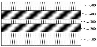
S1: providing a base, the base comprising a substrate, a first insulating layer, an intermediate layer, a second insulating layer and a device layer stacked in sequence from bottom to top;

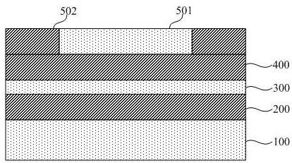
S2: defining a thin film transistor region in the device layer, and forming a device insulating layer around the thin film transistor region;

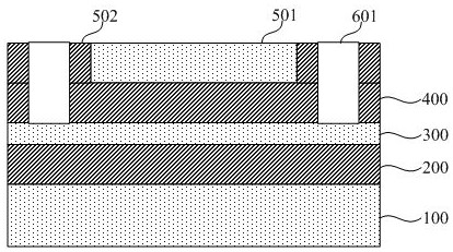
S3: forming a first trench, the first trench penetrates the device insulating layer and the second insulating layer, and exposes the intermediate layer;

S4: forming an intermediate insulating layer at the bottom of the first trench, the intermediate insulating layer passing through the intermediate layer and being in contact with the first insulating layer;

S5 : forming a second trench, the second trench communicates with the first trench, and the second trench penetrates the intermediate ins...


PUM


Abstract

The invention provides an ESD (Electro-Static Discharge) protection device structure for a thin film transistor and a preparation method thereof, and provides a substrate on which a substrate, a first insulating layer, a middle layer, a second insulating layer and a device layer are sequentially stacked from bottom to top, and a first conductive type layer and a second conductive type layer which are in contact with the first insulating layer are formed in the substrate, the ESD protection diode is manufactured on the substrate through the first conductive type layer and the second conductive type layer, a PN junction is formed in the substrate, the PN junction can conduct ESD protection on a thin film transistor circuit manufactured in a device layer in the follow-up process, and due to the fact that the thin film transistor basically belongs to the low-temperature process, the ESD protection diode is manufactured on the substrate through the first conductive type layer and the second conductive type layer. Therefore, the performance degradation of the PN junction in the substrate cannot be caused by the subsequent preparation process of the thin film transistor, and further, when ESD occurs, the middle layer can shield the influence of the leakage current of the PN junction on the thin film transistor, so that the voltage withstanding problem of the ESD protection device structure of the thin film transistor can be effectively solved.

Description

technical field [0001] The invention belongs to the field of semiconductors, and relates to an ESD protection device structure and a preparation method for thin film transistors. Background technique [0002] Static electricity is a phenomenon ubiquitous in nature. When two dielectric materials with different dielectric constants rub against each other, static electricity will be generated along with it. When an object with static electricity is discharged and returns to a neutral state, the phenomenon of electrostatic discharge is called electrostatic discharge (Electrostatic Discharge, ESD). [0003] Due to the high mobility of thin-film channels and good heat dissipation performance, microelectronic device technology based on thin-film channels is considered to be one of the effective ways to improve the performance of integrated circuits. However, due to the small channel region of the thin film, its doping is difficult, resulting in the realization of PN junction in tr...

Claims


Application Information

Patent Timeline
Patent Type & Authority Applications(China)
IPC IPC(8): H01L27/02H01L27/12H01L21/84
CPCH01L27/0255H01L27/1203H01L21/84
Inventor 刘尧刘盛富杨超段花花尹杰刘森
Owner MICROTERA SEMICON (GUANGZHOU) CO LTD
Why Eureka
Try Eureka