Storage element and manufacturing method thereof

A storage element and manufacturing method technology, applied in semiconductor/solid-state device manufacturing, electrical components, semiconductor devices, etc., can solve problems such as gate control failure, and achieve the effect of reducing resistance value and improving gate control.

Pending Publication Date: 2022-06-07
MACRONIX INT CO LTD
View PDF0 Cites 0 Cited by
  • Summary
  • Abstract
  • Description
  • Claims
  • Application Information

AI Technical Summary

Problems solved by technology

Therefore, after the gate replacement process is performed, the topmost word line will have an indented structure between the step region and the array region, resulting in a high-impedance topmost word line, or a string selection line (String Select Line, SSL) gate control failure open problem (openissue)

Method used


Image

  • Storage element and manufacturing method thereof
  • Storage element and manufacturing method thereof
  • Storage element and manufacturing method thereof

Examples


Embodiment Construction

[0080] The present invention will be more fully explained with reference to the accompanying drawings of this embodiment. However, the present invention may also be embodied in various forms and should not be limited to the embodiments described in the present invention. The thicknesses of layers and regions in the figures may be exaggerated for clarity. The same or similar element numbers refer to the same or similar elements, which will not be repeated in the following paragraphs.

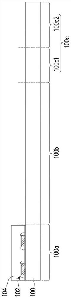
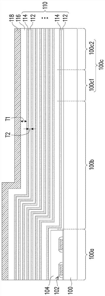
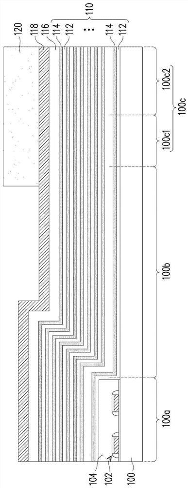
[0081] Figure 1 to Figure 25 A schematic cross-sectional view of a manufacturing process of a memory device according to an embodiment of the present invention.

[0082] Please refer to figure 1 , the storage element 10 (eg Figure 25 shown) manufacturing method is as follows. First, the substrate 100 is provided. In one embodiment, the substrate 100 includes a semiconductor substrate, such as a silicon substrate. The substrate 100 includes a peripheral region 100a, a stepped region 100b,...


PUM


Abstract

The invention discloses a storage element and a manufacturing method thereof, and the storage element comprises a substrate, a laminated structure, a plurality of connecting pads and a protection layer. The substrate has an array region and a step region. The laminated structure is disposed on the substrate. The laminated structure comprises a plurality of dielectric layers and a plurality of conductor layers which are alternately laminated. The pads are disposed on the substrate in the step region. The connecting pads are respectively connected with the conductor layers to form a step structure. The protective layer is disposed on the laminated structure to contact the topmost conductor layer. The top face, close to the topmost connecting pad, of the protection layer is provided with an arc-shaped outline.

Description

technical field [0001] The present invention relates to a semiconductor element and a method of manufacturing the same, and more particularly, to a memory element and a method of manufacturing the same. Background technique [0002] As technology advances, advances in electronic components have increased the need for greater storage capacity. In order to meet the demand for high storage density, memory elements have become smaller in size and higher in integration. Therefore, the types of memory devices have been developed from a two-dimensional memory device (2D memory device) with a planar gate structure to a three-dimensional memory device (3D memory device) with a vertical channel (VC) structure. [0003] Generally speaking, a three-dimensional memory device often uses a conductor layer with a stepped structure as a pad, and uses the pad and the contact window thereon as an interconnect structure, so as to facilitate the connection between the components of each layer a...

Claims


Application Information

Patent Timeline
Patent Type & Authority Applications(China)
IPC IPC(8): H01L27/11521H01L27/11556H01L27/11568H01L27/11582
CPCH10B41/27H10B43/30H10B41/30H10B43/27H10B41/50H10B43/50H01L23/535H01L23/5226H01L23/5283H01L21/76895H01L21/76805H10B41/41H10B43/40
Inventor 王景弘李士勤郑宸语韩宗廷
Owner MACRONIX INT CO LTD
Why Eureka
Try Eureka