Wafer cleaning and drying module state detection method and device and planarization equipment
A state detection and wafer technology, applied in semiconductor/solid-state device manufacturing, image analysis, image enhancement, etc., to reduce possibility, reduce damage probability, improve accuracy and detection efficiency
Pending Publication Date: 2022-06-10
HANGZHOU ZHONGGUI ELECTRONICS TECH CO LTD
View PDF11 Cites 1 Cited by
- Summary
- Abstract
- Description
- Claims
- Application Information
AI Technical Summary
Problems solved by technology
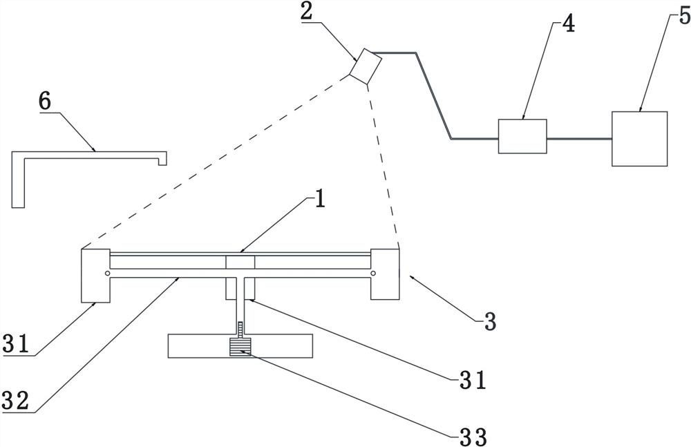
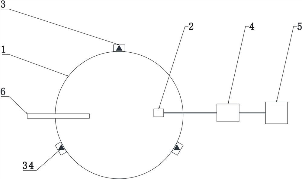
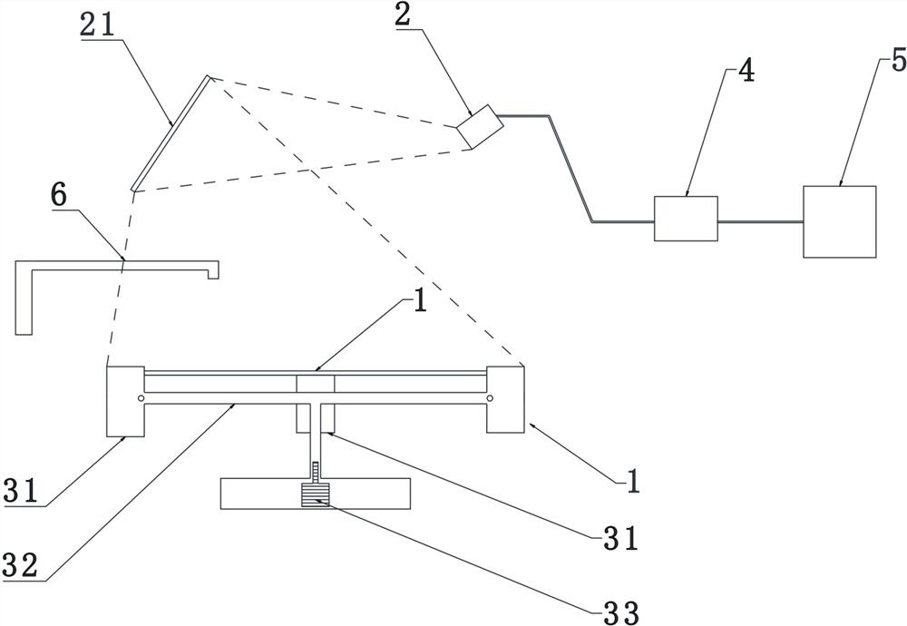
[0003]The current technology is to use two sets of transmissive laser sensors for wafer level detection and one laser ranging sensor for wafer presence detection. This solution is used It will cause problems such as long debugging time, high cost, complex mechanical structure, long detection and feedback time, complex and unsightly device, etc.
In addition, the current technology cannot detect the abnormal state of the wafer gripper, which will cause the tilt of the wafer or the breakage of the wafer when the wafer is placed or taken out under working conditions.
Method used
View moreImage
Smart ImageViewing Examples

Examples
Embodiment Construction
Login to View More PUM
 Abstract
The invention discloses a method for detecting the state of a wafer cleaning and drying module. The method comprises the following steps: acquiring a standard image of a normally placed wafer; preprocessing the standard image to obtain a standard image contour of the normally placed wafer; acquiring parameters of a standard image contour; obtaining a to-be-detected image; preprocessing the to-be-detected image, judging whether a wafer exists or not, and if the wafer exists, obtaining the contour of the to-be-detected image; acquiring parameters of the contour of the to-be-detected image; and comparing the parameters of the to-be-detected image contour with the parameters of the standard image contour, judging whether the difference value is within a set range, and if the difference value exceeds a set threshold value, judging that the wafer is inclined. The invention further discloses a wafer cleaning and drying module state detection device. The invention also discloses chemical mechanical planarization equipment. According to the invention, real-time detection of whether the wafer exists or not and whether the wafer is inclined or not is realized, the detection accuracy is high, and the detection time is short.
Description
technical field [0001] The invention belongs to the technical field of semiconductor processing equipment, and in particular relates to a method and device for detecting the state of a wafer cleaning and drying module, and chemical mechanical planarization equipment provided with the state detecting device. Background technique [0002] The wafer wet cleaning process is to effectively use chemical solution to clean the remaining impurities on the wafer without destroying the surface characteristics and electrical characteristics of the wafer. The wafer wet cleaning process is widely used in chemical mechanical planarization equipment, cleaning equipment and electroplating equipment. Cleaning and drying devices in the existing wafer wet cleaning process, for example, a device that uses spin-drying to dry wafers (Spin Rinse Dry, SRD), or a device that uses IPA to clean and dry wafers, etc. No matter which cleaning and drying method is used, after the wafer is placed, it must ...
Claims
Login to View More Application Information
Patent Timeline
 Patent Type & Authority Applications(China)
IPC IPC(8): G06T7/00G06T7/13G06T7/155G06T7/168G06T7/62H01L21/67
CPCG06T7/001G06T7/13G06T7/155G06T7/168G06T7/62H01L21/67259H01L21/67028G06T2207/20061G06T2207/30148
Inventor 盛思杰
Owner HANGZHOU ZHONGGUI ELECTRONICS TECH CO LTD