Vertically integrated electro-absorption modulated laser and method of manufacture
A technology of absorption modulation and integrated electricity, which is applied in the direction of lasers, semiconductor lasers, laser components, etc., can solve the problems of poor long-term reliability and high price
- Summary
- Abstract
- Description
- Claims
- Application Information
AI Technical Summary
Problems solved by technology
Method used
Image
Examples
Embodiment Construction
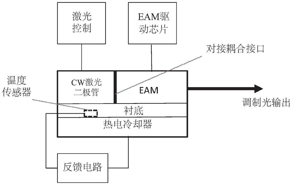
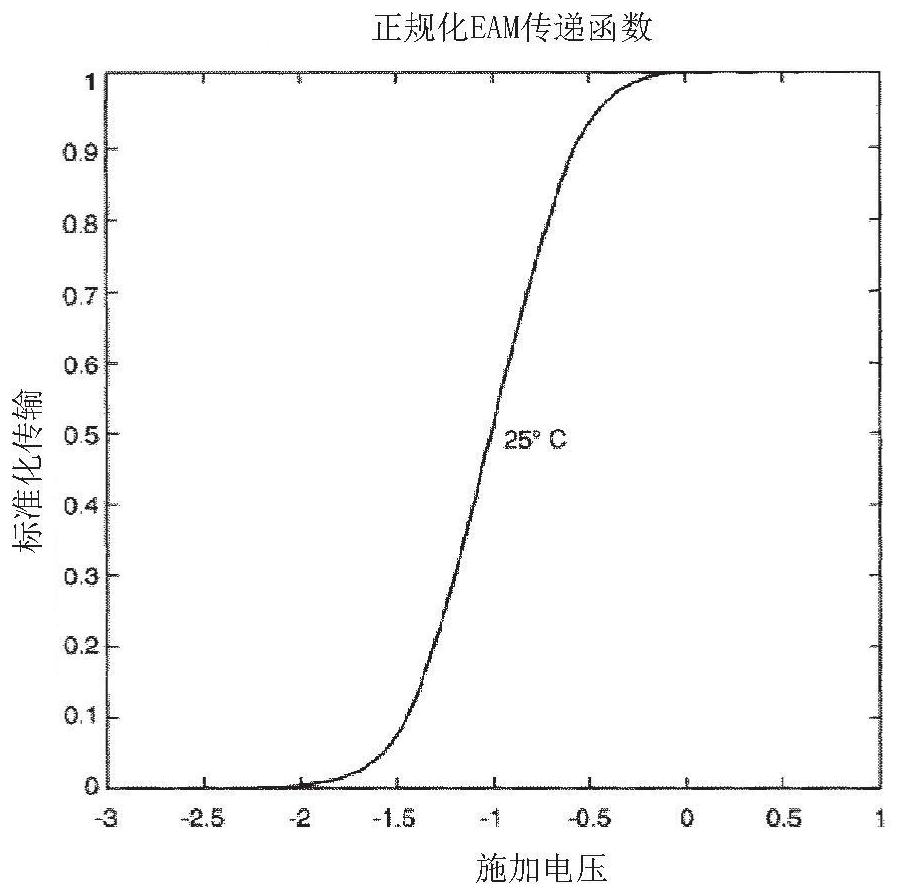
[0113] Figure 1 (Prior Art) shows a schematic block diagram of an example of a butt-coupled EML assembly. The EML assembly consists of a CW laser diode connected to the EAM, mounted on a common substrate, which is backside cooled using a thermoelectric cooler (TEC). Figure 2 (Prior Art) shows a typical normalized transfer function of the EML as shown in Figure 1, ie the normalized transfer of the EAM as a function of applied voltage. In this example, the EAM has 100% transmission at the specified wavelength at zero bias and 0% transmission at -2V reverse bias.
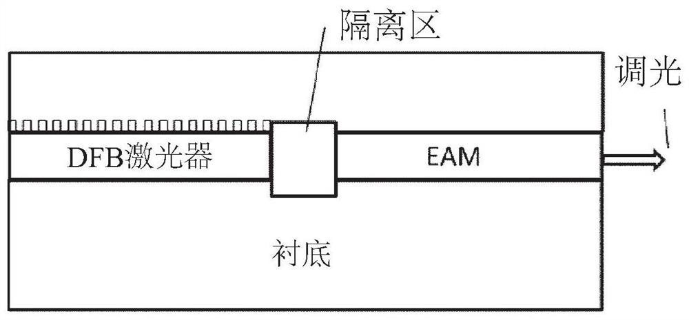
[0114] Figures 3 to 5 (Prior Art) show schematic longitudinal cross-sections (ie through the light propagation axis) of three examples of monolithically integrated EMLs. The EML shown schematically in Figure 3 includes a DFB laser and an EAM fabricated on the same substrate using two different epitaxial layer structures, a waveguide structure for the DFB laser and the EAM, optically coupled through an isolation region...
PUM
 Abstract
Description
Claims
Application Information


