High-end level shift circuit, high-end power control circuit and anti-interference method
A level shift circuit, high-end technology, applied in the direction of eliminating voltage/current interference, controlling/regulating system, adjusting electrical variables, etc., can solve the problems of LDMOS tube manufacturing process influence, power integrated circuit blocking, power integrated circuit burning and other problems
- Summary
- Abstract
- Description
- Claims
- Application Information
AI Technical Summary
Problems solved by technology
Method used
Image
Examples
Embodiment 1
[0041] The high-end level shift circuit and the high-end power control circuit disclosed in the present invention will be further specifically introduced below in combination with the embodiments shown in the accompanying drawings.
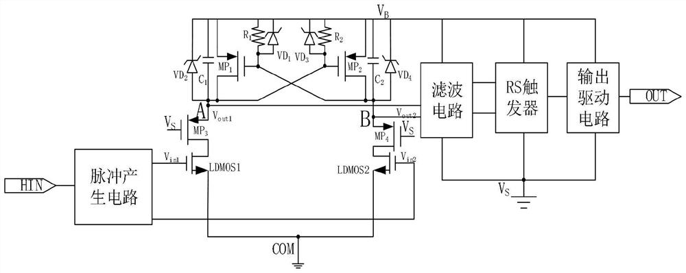
[0042] like figure 1 As shown, the high-end level shift circuit includes a cross-coupled first coupling module and a second coupling module. The first coupling module includes a first LDMOS transistor LDMOS1, a first PMOS transistor MP1, a first capacitor C1, a first resistor R1, a first voltage regulator diode VD1, and a second voltage regulator diode VD2, and the second coupling module includes The second LDMOS transistor LDMOS2 , the second PMOS transistor MP2 , the second capacitor C2 , the second resistor R2 , the third voltage regulator diode VD3 and the fourth voltage regulator diode VD4 .
[0043] The source of the first LDMOS transistor LDMOS1 is grounded, and the drain is connected to the anode of the second Zener diode VD2, the first c...
Embodiment 2
[0051] The high-end level shift circuit and the high-end power control circuit disclosed in the present invention will be further specifically introduced below in combination with the embodiments shown in the accompanying drawings.
[0052] like figure 1 As shown, the high-end power control circuit includes a pulse generation circuit, a filter circuit, an RS flip-flop, an output drive circuit, and the high-end level shift circuit. Wherein, the pulse generating circuit is used to form two low-voltage narrow-pulse working signals; the high-level shift current is used to convert the two low-voltage narrow-pulse working signals into two high-voltage narrow-pulse working signals; the filtering The circuit is used to filter the two high-voltage narrow-pulse working signals to remove the noise signal; the RS flip-flop is used to restore the high-voltage narrow-pulse working signal to a high-voltage wide-pulse working signal; the output drive circuit is used to boost The driving capa...
Embodiment 3
[0056] The anti-jamming method disclosed in the present invention will be further specifically introduced below in combination with the embodiments shown in the accompanying drawings.
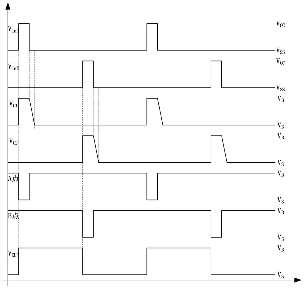
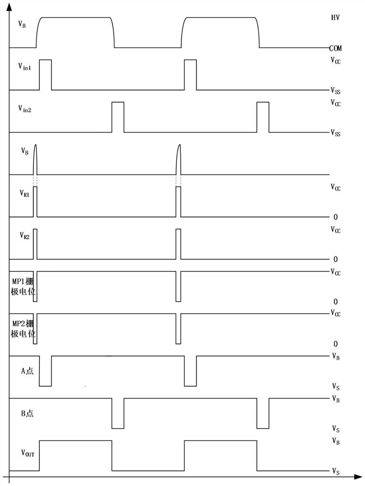
[0057] When the high-end power control circuit is in normal operation, its waveform diagram is as follows figure 2 shown. When the circuit works normally, the source of the third PMOS transistor MP3 is at a high level V B , the third PMOS transistor MP3 is turned on, if the gate input signal Vin1 of the first LDMOS transistor LDMOS1 is at a high level, the first output terminal formed by the first coupling module, that is, the potential at point A will be pulled down from a high level to a low level flat. The first capacitor C1 is in the charging state. When the first LDMOS transistor LDMOS1 is turned on, the first capacitor C1 will be charged to 15V. At the same time, the second PMOS transistor MP2 is turned on. The second output terminal formed by the second coupling module, that is, the p...
PUM
 Abstract
Description
Claims
Application Information


