Method and system for measuring alignment error

An alignment error and measurement technology, applied in the field of alignment error measurement methods and systems, can solve problems such as affecting the performance of semiconductor devices and increasing alignment errors, so as to improve performance, reduce detection time, and improve process performance and productivity effects

Active Publication Date: 2022-06-24
NEXCHIP SEMICON CO LTD
View PDF8 Cites 0 Cited by
  • Summary
  • Abstract
  • Description
  • Claims
  • Application Information

AI Technical Summary

Problems solved by technology

If the entire wafer is compensated with local overlay accuracy, the local alignment error can be reduced, but the alignment error in other directions of the wafer may be further increased, thereby affecting the performance of semiconductor devices

Method used


Image

  • Method and system for measuring alignment error
  • Method and system for measuring alignment error
  • Method and system for measuring alignment error

Examples


Embodiment Construction

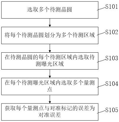
[0048] The technical solutions in the embodiments of the present invention will be clearly and completely described below with reference to the accompanying drawings in the embodiments of the present invention. Obviously, the described embodiments are only a part of the embodiments of the present invention, but not all of the embodiments. Based on the embodiments of the present invention, all other embodiments obtained by those of ordinary skill in the art without creative efforts shall fall within the protection scope of the present invention.

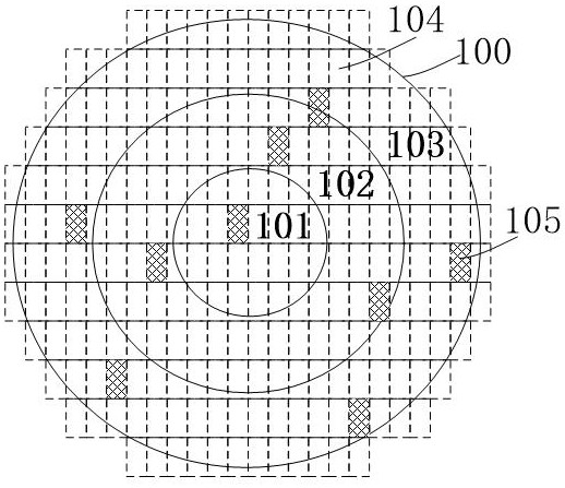
[0049] see figure 1 and image 3 As shown, in the field of semiconductor fabrication technology, a wafer is divided into a number of exposure areas 104, and the exposure area 104 is usually used as a basic unit in production. The exposure areas 104 are periodically repeated on the wafer, and each exposure area 104 includes one or more chips, and the chips are also periodically repeated on the wafer. And a dicing line is arranged bet...


PUM


Abstract

The invention discloses an alignment error measuring method and system, and the method comprises the steps: selecting a plurality of to-be-measured wafers, and enabling the to-be-measured wafers to be provided with a plurality of alignment marks; dividing each wafer into a plurality of to-be-detected areas according to the distance to the center of the to-be-detected wafer; selecting at least one exposure area to be detected in each area to be detected; selecting a plurality of measurement points in each exposure area to be measured, wherein each measurement point is correspondingly provided with the alignment mark on the wafer to be measured; and acquiring an error between each measuring point and the alignment mark as the alignment error. According to the method and the system for measuring the alignment error provided by the invention, the performance and the productivity of the semiconductor device can be improved.

Description

technical field [0001] The invention belongs to the technical field of semiconductor manufacturing, and particularly relates to a method and system for measuring alignment error. Background technique [0002] Semiconductor manufacturing is the process of forming a stacked structure on a substrate through various processes such as photolithography, etching, deposition, and implantation. The correlation between different material layers in the stack structure easily affects the performance of semiconductor devices. In order to improve the performance of the semiconductor device, in the semiconductor manufacturing process, each patterned material needs to be aligned with the previous patterned material layer, that is, the semiconductor process needs to meet a certain overlay accuracy (Overlay). If the alignment error is large, the performance of the semiconductor device is affected, and even the problem of misalignment of the connection layer, which causes a short circuit or d...

Claims


Application Information

Patent Timeline
Patent Type & Authority Applications(China)
IPC IPC(8): G03F7/20
CPCG03F7/70633G03F7/70616G03F7/7085
Inventor 杨学人
Owner NEXCHIP SEMICON CO LTD
Why Eureka
Try Eureka