Decorative plate production process and decorative plate
A production process and technology for decorative panels, which are applied in decorative arts, special decorative structures, processes for producing decorative surface effects, etc., can solve the problems of single visual effect of the appearance pattern of decorative panels, large VOC emissions, and non-environmental protection. Achieve brilliant visual effect, low processing cost and simple preparation process
- Summary
- Abstract
- Description
- Claims
- Application Information
AI Technical Summary
Problems solved by technology
Method used
Image
Examples
Embodiment 1
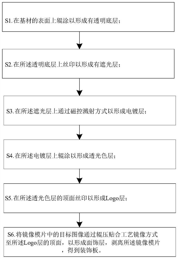
[0037] see figure 1 , Embodiment 1 includes the following steps:
[0038] S1. Roll coating on the surface of the substrate to form a transparent bottom layer, the substrate is a non-transparent substrate, preferably a glass fiber board, and the acrylic resin with a function of 2.3 is applied on the surface of the glass fiber board by roller coating In order to form a transparent bottom layer, the transparent bottom layer is a UV resin layer, and the UV resin is fully contacted with the LED lamp and then cured to obtain a UV photocurable resin layer. The working energy of the LED lamp is 260m / J, so that the UV photocurable resin layer is completely attached to the surface of the glass fiber board. , Strong adhesion, not easy to fall off.
[0039] S2. Screen printing on the transparent bottom layer to form a light-shielding layer. Specifically, the acrylic resin containing a molecular weight of 8000 is screen-printed on the surface of the UV resin layer, and is baked at a tempe...
Embodiment 2
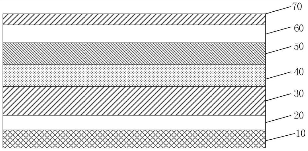
[0051] The difference between the production process of Example 2 and Example 1 is that the decorative board prepared in Example 2 includes: a substrate 10 of a glass fiber board; a transparent bottom layer 20 disposed on the front surface of the substrate 10, and the thickness of the transparent bottom layer 20 is 6 μm The light-shielding layer 30 arranged on the upper surface of the transparent bottom layer 20, the thickness of the light-shielding layer 30 is 13 μm; the electroplating layer 40 arranged on the upper surface of the light-shielding layer 30, the electroplating layer 40 is an indium tin alloy layer; The light-transmitting color layer 50 on the upper surface of the layer 40, the thickness of the light-transmitting color layer 50 is 8 μm; the Logo layer 60 arranged on the upper surface of the light-transmitting color layer 50; and the finishing layer arranged on the surface of the Logo layer 60 70. The surface decoration layer 70 is a texture layer.
Embodiment 3
[0053] The difference between the production process of Example 3 and Example 1 is that the decorative board prepared in Example 3 includes: a substrate 10 of a glass fiber board; a transparent bottom layer 20 arranged on the front surface of the substrate 10, and the thickness of the transparent bottom layer 20 is 8 μm The light-shielding layer 30 arranged on the upper surface of the transparent bottom layer 20, the thickness of the light-shielding layer 30 is 10 μm; the electroplating layer 40 arranged on the upper surface of the light-shielding layer 30, the electroplating layer 40 is an indium tin alloy layer; The light-transmitting color layer 50 on the upper surface of the layer 40, the thickness of the light-transmitting color layer 50 is 1θμm; the Logo layer 60 arranged on the upper surface of the light-transmitting color layer 50; and the finishing layer arranged on the surface of the Logo layer 60 70. The surface decoration layer 70 is a smooth surface layer.
PUM
| Property | Measurement | Unit |
|---|---|---|
| thickness | aaaaa | aaaaa |
| thickness | aaaaa | aaaaa |
| thickness | aaaaa | aaaaa |
Abstract
Description
Claims
Application Information

