Automatic testing device for laser chip

An automatic test and laser technology, which is applied in the direction of measuring devices, measuring device casings, electronic circuit tests, etc., can solve problems such as inconsistency and unstable test data, eliminate fatigue problems, eliminate small rotation offsets, and ensure accuracy Effect

Pending Publication Date: 2022-06-28
STELIGHT INSTR CO LTD
View PDF0 Cites 1 Cited by
  • Summary
  • Abstract
  • Description
  • Claims
  • Application Information

AI Technical Summary

Problems solved by technology

Based on the above findings, the object of the present invention is to provide an automatic testing device for laser chips, which solves the long-term use problem in the prior art due to the fatigue of the test probe assembly on the machine. The problem of unstable and inconsistent test data in the process

Method used


Image

  • Automatic testing device for laser chip
  • Automatic testing device for laser chip
  • Automatic testing device for laser chip

Examples


Embodiment 1

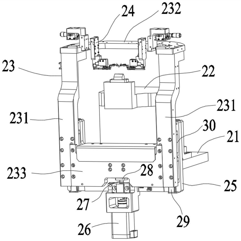
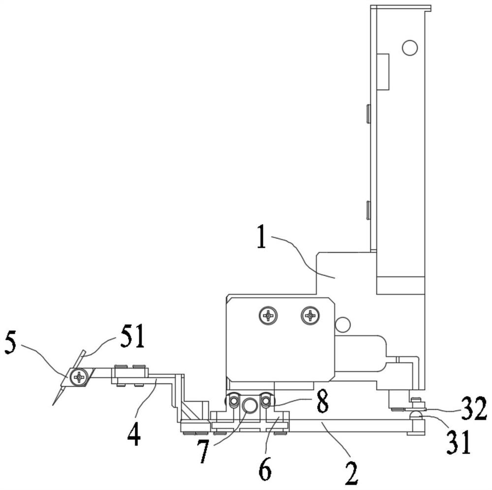
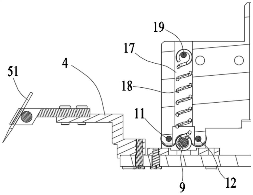
[0024] Embodiment 1: An automated testing device for a laser chip, comprising: a substrate 21, a test table 22 mounted on the upper surface of the substrate 21, a drive bracket 23 mounted on the outside of the substrate 21, and a drive bracket 23 mounted on the test table 22. The upper test probe assembly 24, the test probe assembly 24 includes: a main body 1 connected to the drive bracket 23, a support plate 2, a probe 51 for contacting the chip to be tested, and a moving point contact probe 31, the One end of the support plate 2 is installed with a cantilever 4, the other end is installed with the moving point contact probe 31, and one side of the lower end face of the main body 1 is provided with a static point contact probe 32 located on the upper part of the moving point contact probe 31 and corresponding to it. When the needle is in contact with the chip to be tested, the moving point contact probe rotates with the support plate away from the static point contact probe, t...

Embodiment 2

[0031] Embodiment 2: An automated testing device for a laser chip, comprising: a substrate 21, a test table 22 mounted on the upper surface of the substrate 21, a drive bracket 23 mounted on the outside of the substrate 21, and a drive bracket 23 mounted on the test table 22. The upper test probe assembly 24, the test probe assembly 24 includes: a main body 1 connected to the drive bracket 23, a support plate 2, a probe 51 for contacting the chip to be tested, and a moving point contact probe 31, the One end of the support plate 2 is installed with a cantilever 4, the other end is installed with the moving point contact probe 31, and one side of the lower end face of the main body 1 is provided with a static point contact probe 32 located on the upper part of the moving point contact probe 31 and corresponding to it. One end of the cantilever 4 away from the support plate 2 is fixed with a probe seat 5 on which the probe 51 is installed;

[0032] An adapter seat 6 is installed...


PUM


Abstract

A test probe assembly of the automatic test device comprises a body connected with a driving support, a supporting plate, a probe used for making contact with a chip to be tested and a movable point contact probe, a cantilever is installed at one end of the supporting plate, and the movable point contact probe is installed at the other end of the supporting plate. One side of the lower end face of the body is provided with a static point contact probe which is located on the upper portion of the movable point contact probe and corresponds to the movable point contact probe, one end, away from the supporting plate, of the cantilever is fixedly provided with a probe seat provided with the probe, the probe seat comprises a base and a clamping piece, the probe is located between the base and the clamping piece, and the included angle between the probe and the supporting plate is 30 degrees. According to the invention, the stability, repeatability, comparability and consistency of detection data are improved.

Description

technical field [0001] The invention relates to an automatic testing device for laser chips, belonging to the technical field of chip testing. Background technique [0002] In the production and testing of lasers in the optical communication industry, before the COC aging process, the optoelectronic performance test of a single laser chip (Laser Diode, LD) is also required. During the test of a single laser chip (LD) in optical communication, the probe Stability plays a very important role. Since the size of a single chip is very small (generally in the range of 300μm), the test probe will more or less push the position or angle of the chip during the process of contacting the chip. Once the position of the chip is Changes in angle and angle will directly affect the stability of subsequent test indicators and test efficiency, and the pressure stability of the test probe will also be directly fed back to the stability of the test value. For mass production testing, a probe T...

Claims


Application Information

Patent Timeline
Patent Type & Authority Applications(China)
IPC IPC(8): G01R31/28G01R1/04G01R1/067
CPCG01R31/2886G01R31/2887G01R1/04G01R1/06705
Inventor 黄建军吴永红赵山胡海洋
Owner STELIGHT INSTR CO LTD
Why Eureka
Try Eureka