

Instruction programmable buffer design system based on processor debugging architecture
A technology for designing systems and processors, applied in the field of instruction programmable buffer design systems, can solve problems such as differences in results and processor interruptions, and achieve the effects of simple structure, high flexibility, and easy operation
- Summary
- Abstract
- Description
- Claims
- Application Information
AI Technical Summary
Problems solved by technology
Method used
Image

Examples
Embodiment Construction
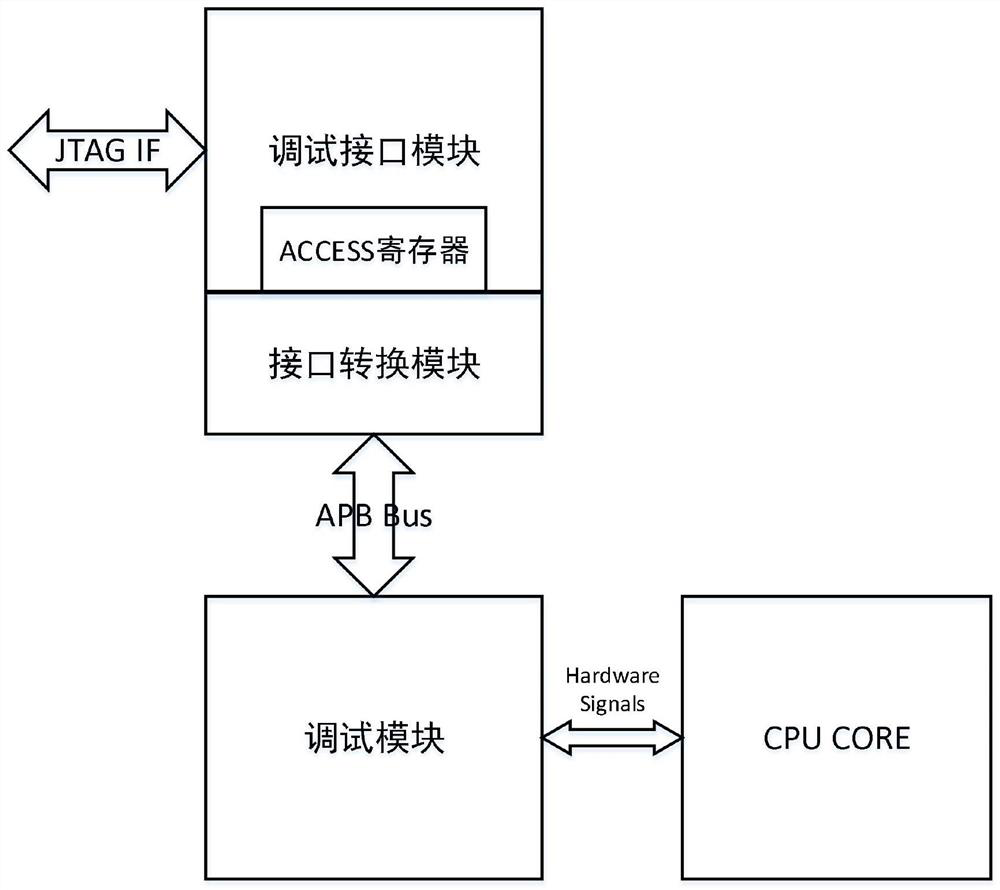
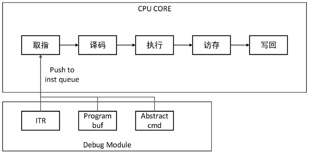
[0020] like figure 1 As shown in the block diagram of the architecture, this embodiment provides an instruction programmable buffer design system based on the processor debugging architecture. The processor core system built in the design system is the basic framework of the application, serving the instruction programmable buffer. The processor core system includes a debug interface module, an interface conversion module, and a debug module, wherein an instruction programmable buffer design is added to the hardware design of the debug module to provide software debuggers with downloading instructions to the processor core in the debug mode. the means of execution;
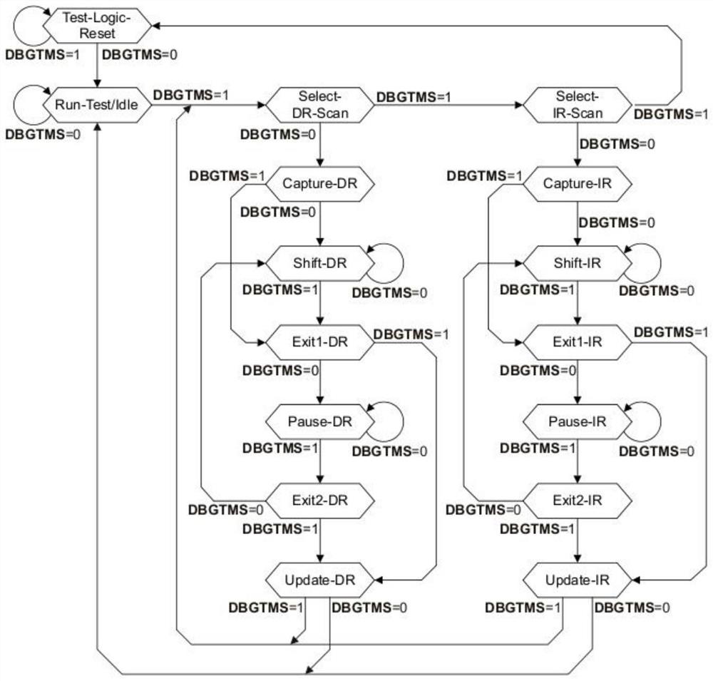
[0021] The debug interface module implements the JTAG interface conforming to the IEEEStd 1149.1-2013 protocol standard, including five interface signals of TCK, nRESET, TMS, TDI and TDO. TCK and nRESET are clock and reset, TMS is used for controller JTAG state machine jump, TDI and TDO are serial input and outpu...
PUM
 Abstract
Description
Claims
Application Information