Method for measuring etching deviation of hard mask layer in self-alignment imaging process

A technology of hard mask layer and measurement method, which is applied in semiconductor/solid state device testing/measurement, electrical components, circuits, etc. problems, to reduce defects, reduce the influence of random factors, and improve accuracy

Pending Publication Date: 2022-07-01
SHANGHAI HUALI INTEGRATED CIRCUTE MFG CO LTD
View PDF0 Cites 0 Cited by
  • Summary
  • Abstract
  • Description
  • Claims
  • Application Information

AI Technical Summary

Problems solved by technology

[0004] In view of the above-mentioned shortcomings of the prior art, the purpose of the present invention is to provide a method for measuring the etching deviation of the hard mask layer in the self-aligned imaging process, which is used to solve the problem of the three-dimensional structure of the bottom layer in the prior art. The shear layer of fin does not leave imprints on the bottom layer after the etching process, so it is impossible to directly measure the critical dimensions after development, and it is impossible to obtain the etching deviation and its impact on fin damage, and it is impossible to simulate the chip The problem of real etching behavior in

Method used


Image

  • Method for measuring etching deviation of hard mask layer in self-alignment imaging process
  • Method for measuring etching deviation of hard mask layer in self-alignment imaging process
  • Method for measuring etching deviation of hard mask layer in self-alignment imaging process

Examples


Embodiment Construction

[0039] The embodiments of the present invention are described below through specific specific examples, and those skilled in the art can easily understand other advantages and effects of the present invention from the contents disclosed in this specification. The present invention can also be implemented or applied through other different specific embodiments, and various details in this specification can also be modified or changed based on different viewpoints and applications without departing from the spirit of the present invention.

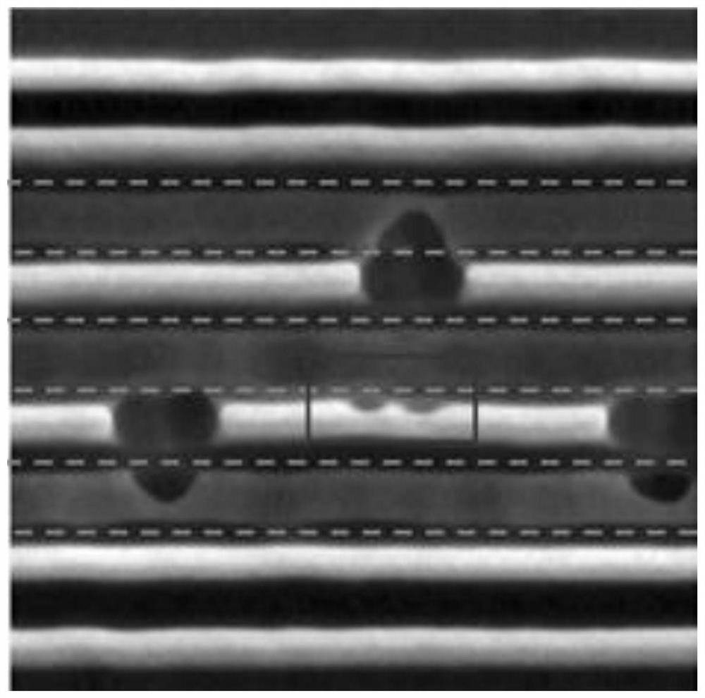
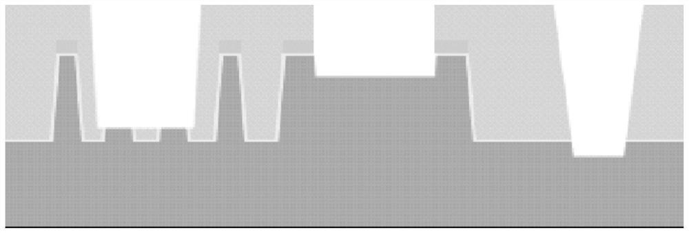
[0040] see Image 6 , the present invention provides a method for measuring the etching deviation of a self-aligned imaging process hard mask layer, comprising:

[0041] Step one, see Figure 3 to Figure 5 , design the main layout, the main layout includes the sacrificial layer pattern 20 (Mandrel) distributed at equal intervals in the X direction, the sacrificial layer pattern 20 (Mandrel) distributed in sequence with a fixed offset in the...


PUM


Abstract

The invention provides a method for measuring the etching deviation of a shear layer in a self-alignment imaging process, and the method comprises the steps: designing a test pattern, and a main layout comprises sacrificial layer patterns which are distributed at equal intervals in the X direction and are sequentially distributed at fixed offset in the Y direction, and a plurality of rows of shear layer patterns which are distributed at equal intervals in the X and Y directions. And the period of two adjacent sacrificial layer patterns in each column in the Y direction is consistent with the period of the shear layer pattern. And transferring the test pattern to a photomask, carrying out a series of processes such as photoetching and etching, carrying out detection by using a large-field detection tool, and determining the boundary of the etched pattern through the fin structure which is just completely cut off and the position of the fin structure which is just cut off. According to the method, the boundary of the shearing layer AEI CD is accurately determined, so that the etching deviation is determined, reference is provided for adjustment of an optical proximity effect correction / photoetching / etching process, the accuracy of process correction and adjustment is improved, and defects are reduced.

Description

technical field [0001] The invention relates to the technical field of semiconductors, in particular to a method for measuring the etching deviation of a hard mask layer in a self-aligned imaging process. Background technique [0002] In the FinFet (fin transistor) process, the SADP (Self-Aligned Dual Imaging) process is used to define the overall fin, and then the redundant fin is removed by shearing layers parallel to the fin and perpendicular to the fin to define the active Area. For shear layers parallel to the fin, the ideal is to etch away the excess integral fin without damaging the upper and lower fins. like figure 1 , are the overall fin and the active area defined by the shear layer, respectively, the dotted line marked area is the shear layer area parallel to the fin, and the fin near the boundary of the shear layer has obvious fin damage. [0003] From the layout file to the final active area, through OPC (Optical Proximity Effect) correction, photolithography...

Claims


Application Information

Patent Timeline
Patent Type & Authority Applications(China)
IPC IPC(8): H01L21/336H01L21/66
CPCH01L22/12H01L22/20H01L29/66795
Inventor 钱睿赖璐璐刘必秋张聪
Owner SHANGHAI HUALI INTEGRATED CIRCUTE MFG CO LTD
Why Eureka
Try Eureka