Check patentability & draft patents in minutes with Patsnap Eureka AI!

Method and device for determining alignment mark of wafer

A technology for aligning marks and determining methods, used in semiconductor/solid-state device parts, semiconductor devices, electrical components, etc., can solve the problems of reducing the production efficiency of production chips, long moving distances, etc., and achieves the goal of improving efficiency and reducing costs. Effect

Pending Publication Date: 2022-07-01
BEIJING SEMICON EQUIP INST THE 45TH RES INST OF CETC
View PDF0 Cites 0 Cited by
  • Summary
  • Abstract
  • Description
  • Claims
  • Application Information

AI Technical Summary

Problems solved by technology

However, this selection method will make the movement distance of the moving table carrying the wafer relatively long, reducing the production efficiency of producing chips

Method used


Image

  • Method and device for determining alignment mark of wafer
  • Method and device for determining alignment mark of wafer
  • Method and device for determining alignment mark of wafer

Examples


Embodiment Construction

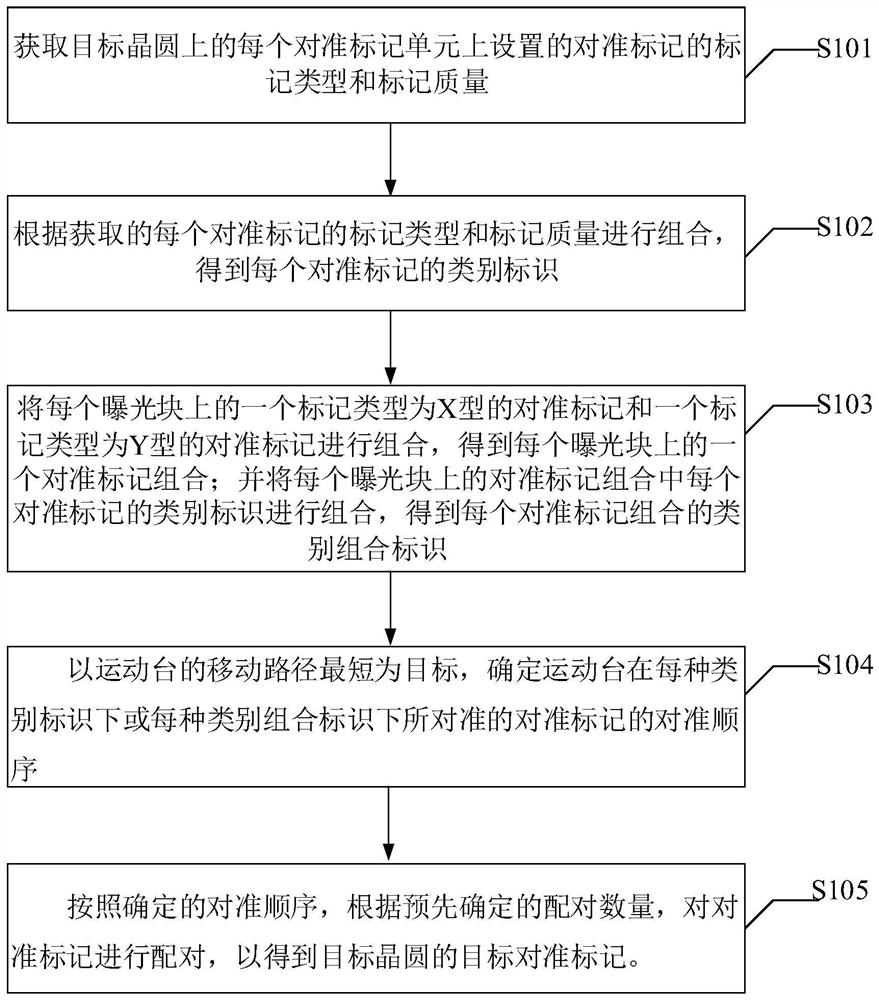
[0052] In order to make the purposes, technical solutions and advantages of the embodiments of the present application more clear, the technical solutions in the embodiments of the present application will be clearly and completely described below with reference to the accompanying drawings in the embodiments of the present application. Obviously, the described embodiments are only It is a part of the embodiments of the present application, but not all of the embodiments. The components of the embodiments of the present application generally described and illustrated in the drawings herein may be arranged and designed in a variety of different configurations. Thus, the following detailed description of the embodiments of the application provided in the accompanying drawings is not intended to limit the scope of the application as claimed, but is merely representative of selected embodiments of the application. Based on the embodiments of the present application, all other embo...


PUM


Abstract

The invention provides a wafer alignment mark determination method and device, and the method comprises the steps: obtaining the mark type and the mark quality of an alignment mark disposed on each alignment mark unit on a target wafer; performing combination according to the obtained mark type and mark quality of each alignment mark to obtain a category identifier of each alignment mark; determining a category combination identifier of each alignment mark combination; determining an alignment sequence of the alignment marks aligned by the motion table under each category identifier or each category combination identifier by taking the shortest moving path of the motion table as a target; and according to the determined alignment sequence and a predetermined pairing number, pairing the alignment marks to obtain a target alignment mark of the target wafer. Through the determination method and the determination device, the alignment mark which enables the wafer workbench to move by a smaller distance can be selected, so that the chip production efficiency is improved, and the cost required by chip production is reduced.

Description

technical field [0001] The present application relates to the field of integrated circuit manufacturing, and in particular, to a method and a device for determining an alignment mark of a wafer. Background technique [0002] In the field of integrated circuit manufacturing, printing the pattern on the mask onto the wafer according to a certain proportion through semiconductor process equipment is the most critical process for manufacturing chips. In this process, due to the uneven surface of the wafer and the alignment deviation of the equipment, a certain deviation will occur when the pattern on the mask is printed on the wafer during the exposure process. Therefore, It is usually necessary to determine the surface shape data of the wafer surface through the alignment marks on the wafer, so that the pattern on the mask can be accurately printed on the corresponding position of the wafer according to the surface shape data. [0003] In the conventional selection method of t...

Claims


Application Information

Patent Timeline
IPC IPC(8): H01L21/68H01L23/544
CPCH01L23/544H01L21/681H01L2223/54426
Inventor 苏鹏方杜旭高荣荣曲越奇张香兰
Owner BEIJING SEMICON EQUIP INST THE 45TH RES INST OF CETC
Features
  • R&D
  • Intellectual Property
  • Life Sciences
  • Materials
  • Tech Scout
  • Unparalleled Data Quality
  • Higher Quality Content
  • 60% Fewer Hallucinations
Learn More