Semiconductor device and preparation method thereof

A technology for semiconductors and devices, applied in the field of semiconductor devices and their preparation, can solve problems such as short circuits, semiconductor devices cannot be used normally, and achieve the effect of avoiding short circuits and stable performance.

Pending Publication Date: 2022-07-01
DYNAX SEMICON
View PDF0 Cites 0 Cited by
  • Summary
  • Abstract
  • Description
  • Claims
  • Application Information

AI Technical Summary

Problems solved by technology

[0003] However, because the patch silver paste will cause the electrochemical migration of silver ions under the action of an electric field, the silver ions will migrate to the front of the

Method used


Image

  • Semiconductor device and preparation method thereof
  • Semiconductor device and preparation method thereof
  • Semiconductor device and preparation method thereof

Examples


Embodiment Construction

[0049] The present invention will be further described in detail below in conjunction with the accompanying drawings and embodiments. It should be understood that the specific embodiments described herein are only used to explain the present invention, but not to limit the present invention. In addition, it should be noted that, for the convenience of description, the drawings only show some but not all structures related to the present invention.

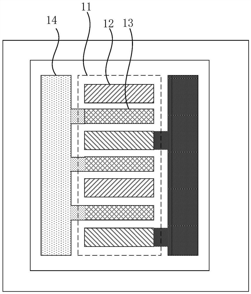
[0050] figure 1 is a schematic structural diagram of a semiconductor device in the prior art, such as figure 1 As shown, the semiconductor device includes a source electrode 12 and a gate electrode 13 located in the active region 11, and a gate bonding pad 14 located in the passive region. The gate bonding pad 14 is electrically connected to the plurality of gate electrodes 13, and the source electrode 12 is electrically connected to the source back electrode (not shown in the figure) through vias. When the semiconductor device ...


PUM


Abstract

The embodiment of the invention discloses a semiconductor device and a preparation method thereof. The semiconductor device comprises a working region and a scribing region surrounding the working region, the working area comprises an active area and a passive area surrounding the active area; the semiconductor device further comprises a substrate, a plurality of semiconductor layers, a grid electrode, a grid electrode bonding disc and a shielding structure. The grid electrode bonding disc is electrically connected with the grid electrode; by additionally arranging the shielding structure, silver ions in patch silver paste in the packaging process are effectively shielded from being migrated to the bonding disc, it is guaranteed that the bonding disc and the electrode connected with the bonding disc are stable in performance, the bonding disc and the electrode connected with the bonding disc are prevented from being short-circuited with the source electrode, and it is guaranteed that the semiconductor device can work normally.

Description

technical field [0001] Embodiments of the present invention relate to the technical field of semiconductors, and in particular, to a semiconductor device and a method for fabricating the same. Background technique [0002] After the semiconductor chip is prepared, the semiconductor chip needs to be packaged to form a semiconductor device. The semiconductor device is generally packaged by the patch method, and because the cost of the patch silver paste in the semiconductor device patch method is low, the patch silver paste method is generally used to connect some of the metal connection electrodes in the semiconductor device through the paste. The silver paste is electrically connected to the metal electrodes in the package casing. [0003] However, because the patch silver paste will cause the electrochemical migration of silver ions under the action of the electric field, the silver ions will migrate to the front side of the semiconductor chip, and contact with other elect...

Claims


Application Information

Patent Timeline
IPC IPC(8): H01L29/778H01L21/335H01L29/40
CPCH01L29/778H01L29/66462H01L29/408
Inventor 裴轶韩啸李元
Owner DYNAX SEMICON
Why Eureka
Try Eureka